논문/REGULAR PAPERS
Out-Phased Current Combining 방식과 Complex Combining Load 방식을 이용한 3.7~4.0 GHz 대역 GaN-HEMT Doherty 전력증폭기
최재혁
,
진일비,
김성형,
송재성,
이윤정,
임서균,
양영구†
3.7~4.0 GHz GaN-HEMT Doherty Power Amplifier Using Out-Phased Current Combining and Complex Combining Load Methods
Jaehyuk Choi,
Yifei Chen,
Seong-Hyoung Kim,
Jaeseong Song,
Yoonjung Lee,
Seogyun Lim,
Youngoo Yang†
Author Information & Copyright ▼
Department of Electrical and Computer Engineering, Sungkyunkwan University
© Copyright 2023 The Korean Institute of Electromagnetic Engineering and Science. This is an Open-Access article distributed under the terms of the
Creative Commons Attribution Non-Commercial License (http://creativecommons.org/licenses/by-nc/4.0/) which permits
unrestricted non-commercial use, distribution, and reproduction in any
medium, provided the original work is properly cited.
Received: Sep 27, 2023; Revised: Oct 16, 2023; Accepted: Oct 24, 2023
Published Online: Nov 30, 2023
요 약
본 논문은 OCC(out-phased current combining)와 CCL(complex combining load)을 함께 적용하여 확장된 OBO(output power back-off)를 가지는 DPA(Doherty power amplifier)를 제안한다. OCC나 CCL을 단독으로 적용할 경우 carrier 증폭기의 출력 임피던스가 하나의 값으로 결정된다. 반면, OCC와 CCL을 함께 적용하면 carrier 증폭기의 출력 임피던스를 선택할 수 있게 되어 회로 설계에 자유도가 생긴다. 제작된 DPA는 carrier 증폭기의 load impedance 변조비를 기존의 2배에서 5배로 확장하여 확장된 back-off 영역을 얻었다. 제작된 DPA는 3.7~4.0 GHz에서 CW 신호를 이용하여 43.0~44.3 dBm의 출력전력, 8.0~8.5 dB의 gain을 얻었다. Peak power에서 72.5~77.9 %의 DE, 9 dB OBO에서 41.5~48.4 %의 DE를 얻었다. 7.8 dB의 PAPR(peak-to-average power ratio)을 갖는 5G NR 100 MHz 64-QAM OFDM 신호를 이용하여 8.2~8.7 dB의 gain과 9 dB OBO에서 45.6~50.0 %의 DE, −22.0~−26.6 dBc의 ACLR을 얻었다.
Abstract
This paper proposes a Doherty power amplifier (DPA) with an extended output power back-off (OBO) using out-phased current combining (OCC) and complex combining load (CCL) methods. When OCC or CCL is applied independently, the output impedance of the carrier amplifier is determined to be a single value. However, when OCC and CCL are applied together, the output impedance of the carrier amplifier can be selected, which provides freedom in the circuit design. The implemented DPA achieves an extended back-off region by expanding the load impedance modulation ratio of the carrier amplifier by five times between the low-power and peak-power levels. The implemented DPA achieves 43.0~44.3 dBm output power and 8.0~8.5 dB gain using a CW signal at 3.7~4.0 GHz. It achieves 72.5~77.9 % DE at peak power and 41.5~48.4 % DE at 9 dB OBO. Furthermore, it achieves 8.2~8.7 dB of gain, 45.6~50.0 % DE at 9 dB OBO, and an ACLR of −22.0~−26.6 dBc using a 100 MHz 64-QAM 5G NR modulated signal with a peak-to-average power ratio (PAPR) of 7.8 dB.
Keywords: Out-Phased Current Combining; Complex Combing Load; Doherty Power Amplifier; Extended Output Back-Off
I. 서 론
무선통신이 발전함에 따라 변조 신호의 높은 PAPR (peak-to-average power ratio)로 인해 전력증폭기의 평균 출력전력에서의 효율이 중요해지고 있다. 따라서 output power back-off 영역에서의 효율을 높이기 위해 DPA (Doherty power amplifier)가 사용되고 있다[1]~[17]. 기본적인 구조의 DPA는 6 dB의 OBO(output power back-off)를 가진다. PAPR이 증가함에 따라 더 확장된 OBO에서 증폭기 효율의 개선이 필요하다. 더 확장된 OBO를 가지기 위해 asymmetric DPA, CCL(complex combing load), VS(virtual stub), OCC(out-phased current combining)와 같은 연구들이 진행되고 있다[3]~[17].
그 중 OCC은 높은 출력 전력에서 전력 결합 node에서 carrier 증폭기와 peaking 증폭기의 출력 전류의 위상 차이를 조절함으로써 OBO 영역을 확장하는 방식이다. CCL은 증폭기 부하 임피던스에 허수부 성분을 도입함으로써 OBO 영역을 확장하는 방식이다.
본 논문에서는 Cree사의 GaN-HEMT 소자인 CG2H40010F 를 사용하여 DPA를 설계하였다. OBO 영역을 확장하기 위해 OCC와 CCL을 함께 적용하여 전력 결합 node에서의 impedance가 허수부를 가지며, carrier 증폭기와 peaking 증폭기의 전류가 위상 차이를 가지도록 설계하였다.
Ⅱ. 제안하는 Doherty 전력증폭기
9 dB의 OBO를 얻기 위한 설계 파라미터들은 참고문헌 [14]의 수식을 이용하여 구할 수 있다. 먼저, 식 (1)에서 k는 carrier amp의 low power와 peak power에서의 전력비다.
Carrier 증폭기의 low power와 peak power에서의 전력비를 이용하여 symmetric DPA의 OBO를 식 (2)와 같이 구할 수 있다.
Coventional DPA의 k는 2로 6 dB의 OBO를 가진다. OBO를 확장하기 위해선, 더 큰 k를 가져야 한다.
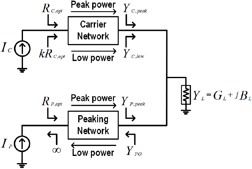
GL과 BL은 그림 1에서 admittance YL의 conductance와 susceptance이다. BPO는 low power에서 peaking amplifier의 admittance인 YPO의 susceptance이다. QL과 QPO는 각각 combining load와 peaking amplifier에 대한 설계 파라미터로 식 (3) 및 식 (4)와 같이 정의한다.
YC,peak와 YP,peak는 그림 1에서 peak power에서의 carrier 증폭기와 peaking 증폭기의 load admittance로 식 (5) 및 식 (6)과 같다.
YC,low는 그림 1에서 low power에서 carrier 증폭기의 load admittance로 식 (7)과 같다. YPO는 그림 1에서 low power에서 carrier 증폭기의 load admittance로 식 (7)과 같다.
OCC를 사용할 경우 식 (9)와 같이 peak power에서 ZC,peak와 ZP,peak의 실수부와 허수부의 비율이 같아야 한다[16]. CCL을 사용할 경우와 식 (10)와 같이 ZL이 허수부를 가지게 된다[9].
c가 식 (11)과 같이 정의될 때 식 (5)~식 (8)이 식 (9) 및 식 (10)을 만족시키기 위해선 QL과 QPO가 표 1의 값을 가진다. RL이 결정되면 OCC나 CCL을 단독 사용하는 경우 QL과 QPO가 하나의 값으로 결정되어 출력 네트워크의 임피던스들이 각각 하나의 값으로 결정된다. 이 경우 결정된 임피던스들을 이용하여 설계할 경우 네트워크 설계가 복잡해질 수 있다. 하지만, OCC와 CCL을 함께 사용할 경우 QL을 특정 범위 내에서 적절하게 선택할 수 있어 네트워크 설계의 자유도가 생기게 된다.
표 1. | Table 1.
설계 파라미터 | Design parameters.
| Combination |
QL
|
QPO
|
| OCC |
0 |
0 |
| CCL |
−2 c |
0 |
| OCC+CCL |
(−3 c, 0) |
0 |
Download Excel Table
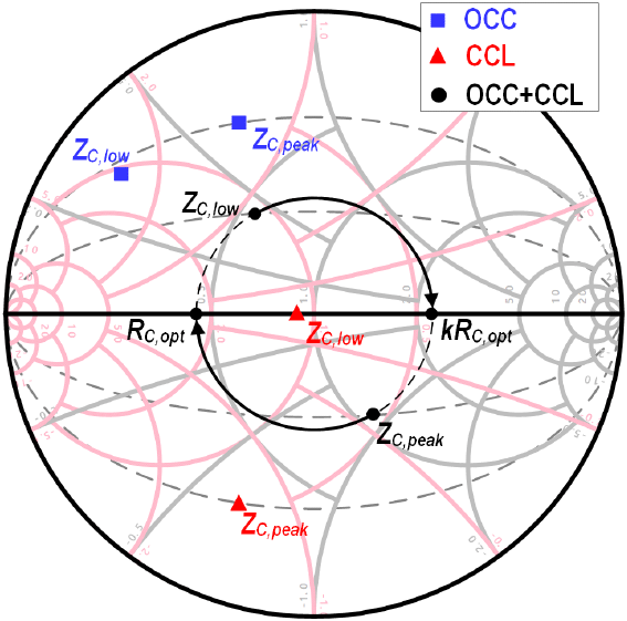
그림 2는 표 1의 설계 파라미터를 이용하여 low power와 peak power에서의 carrier 증폭기의 load impedance를 smith chart에 표현한 것이다. OCC와 CCL을 함께 사용할 경우 네트워크 설계를 고려하며 적절한 QL을 선택하여 작은 Q circle 안에서 carrier network의 임피던스 변환이 되도록 할 수 있다.
그림 2. | Fig. 2.
낮은 전력과 피크 전력에서 carrier 증폭기 출력 네트워크의 임피던스()에 의해 정규화) | Load impedances of carrier amplifier in low power and peak power (normalized by ).
Download Original Figure
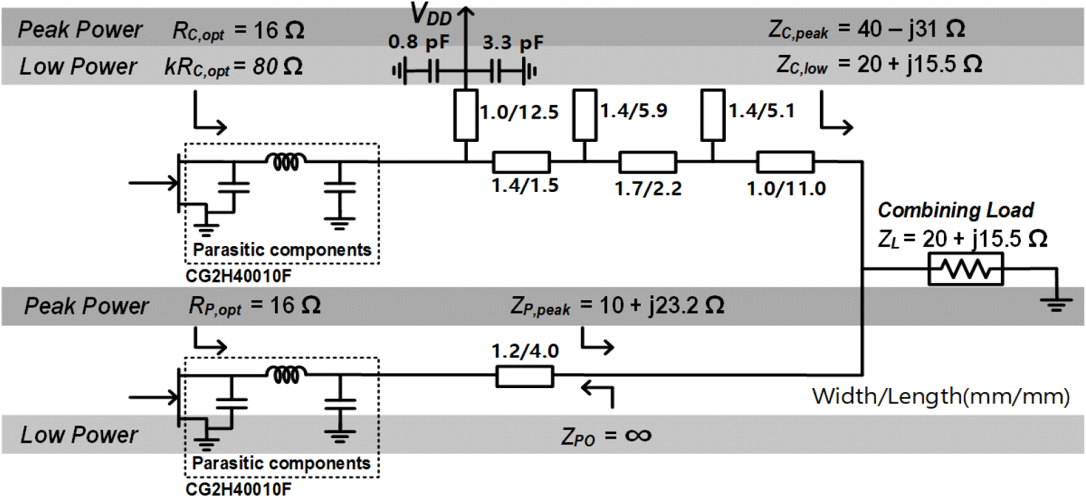
그림 3에서 RC,opt와 RP,opt는 load-pull simulation을 통해 찾은 carrier 증폭기와 peaking 증폭기의 최적 impedance이다. Load-pull simulation을 통해 RC,opt와 RP,opt를 각각 16 Ω으로 결정하였다. 식 (2)를 이용하여 10 dB의 확장된 OBO를 얻기 위해 k의 값은 5로 선택하였다. QL을 −0.667 c로 설정하여 low power와 peak power에서의 load impedance가 작은 Q circle 안에 있도록 하였다. 이때 carrier 증폭기와 peaking 증폭기의 low power와 peak power에서의 load impedance를 그림 3과 같이 구하였다.
Ⅲ. 설계 및 측정
Carrier 증폭기의 경우 low power에서 ZC,low에서 RC,opt로 impedance matching이 되고, peak power에서 ZC,peak에서 kRC,opt로 impedance matching되는 carrier load network를 설계하였다.
Peaking 증폭기의 경우 ZP,peak에서 RP,opt로 impedance matching이 되고 동시에 ZPO가 open(∞)이 되는 peaking load network를 설계하였다.
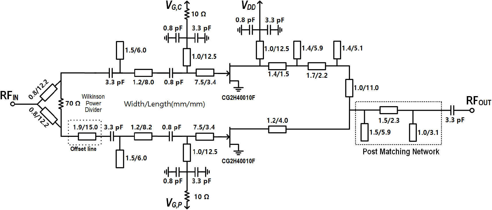
그림 4는 본 논문에서 설계한 DPA의 전체 회로도와 제작된 DPA를 보여준다. Carrier 증폭기와 peaking 증폭기 모두 Cree의 GaN-HEMT CG2H40010F를 사용하였다. 입력 신호는 50 Ω에서 30 Ω으로 임피던스 변환하는 Wilkinson Power Divider를 통해 동일하게 분배된다. Carrier 증폭기와 peaking 증폭기 모두 같은 구조의 입력단의 회로를 사용하였으며, 입력 회로 앞 단에 offset line을 사용하여 출력 전류의 위상 차이를 조절하였다.
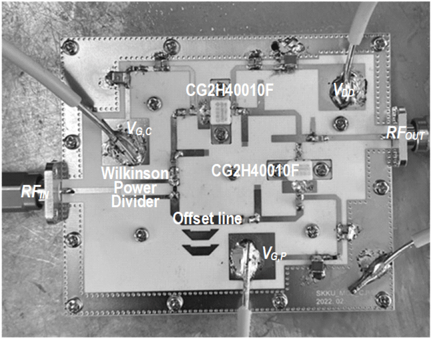
그림 5는 제작된 DPA의 사진이다. PCB는 Rogers RO4350B가 사용되었다. 전체 회로의 크기는 7.1×6.0 cm2이다. Carrier 증폭기와 peaking 증폭기의 gate voltage는 각각 −2.9 V와 −7 V가 사용되었고, drain voltage는 하나의 drain bias 회로를 통해 28 V가 인가되었다.
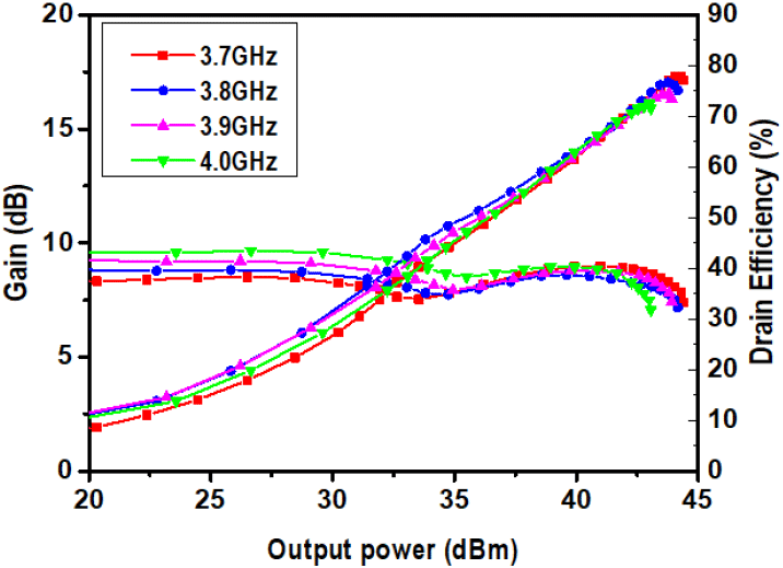
그림 6은 3.7~4.0 GHz 대역에서 CW 신호를 이용하여 측정한 제작된 DPA의 gain과 DE를 나타낸다. 제작된 DPA는 43.0~44.3 dBm의 peak power, 8.0~8.5 dB의 gain을 얻었다. 또한, peak power에서 72.5~77.9 %의 DE, 9 dB OBO에서 41.5~48.4 %의 DE를 얻었다.
그림 6. | Fig. 6.
3.7~4.0 GHz 대역에서 CW 신호를 이용하여 측정한 제작된 DPA의 성능 | Measured performances using a CW signal for the frequency band 3.7~4.0 GHz.
Download Original Figure
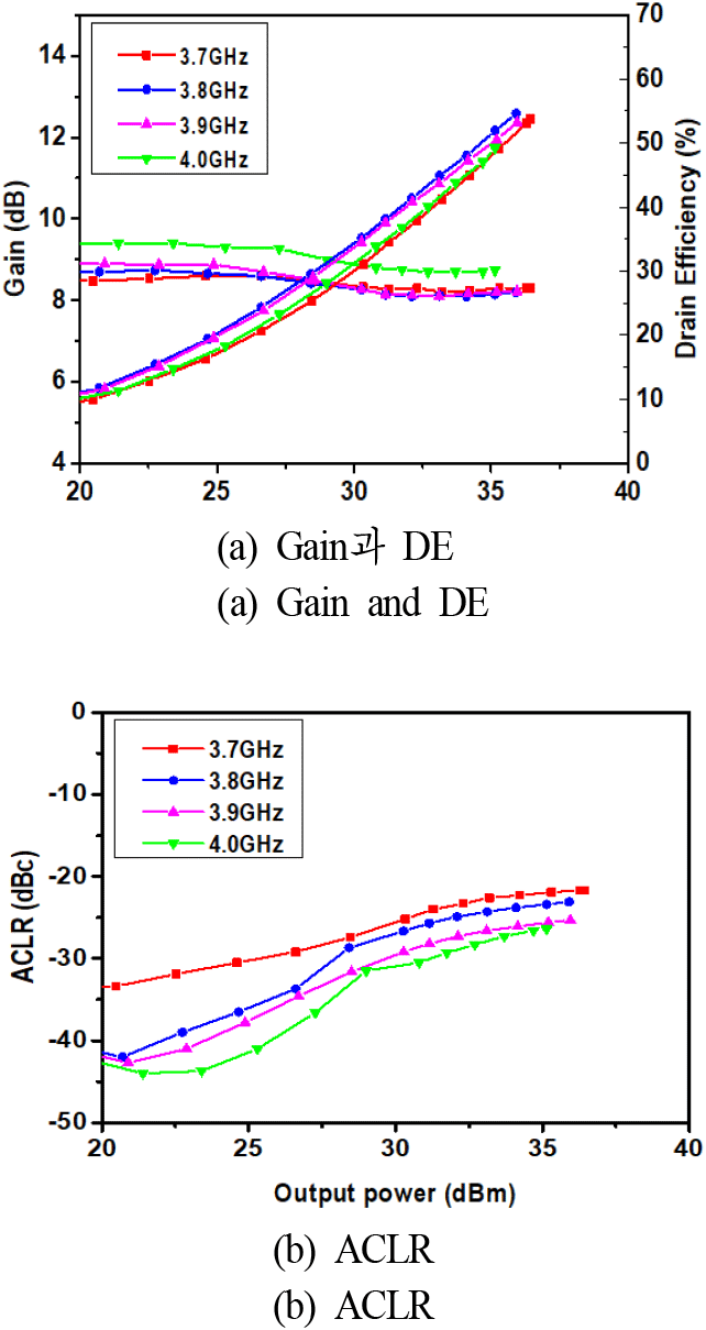
그림 7은 7.8 dB의 PAPR을 갖는 5G NR 100 MHz 64-QAM OFDM 신호를 이용하여 측정한 제작된 DPA의 gain, DE와 ACLR 성능을 나타낸다. 제작된 DPA는 3.7~4.0 GHz 대역에서 8.2~8.7 dB의 gain과 9 dB OBO에서 45.6~50.0 %의 DE를 얻었고, 9 dB OBO에서 −22.0~−26.6 dBc의 ACLR을 얻었다.
그림 7. | Fig. 7.
7.8 dB의 PAPR을 갖는 5G NR 100 MHz 64-QAM OFDM 신호를 이용하여 측정한 제작된 DPA의 성능 | Measured performances of the implemented DPA using a 5G NR 100 MHz 64-QAM OFDM with a PAPR of 7.8 dB.
Download Original Figure
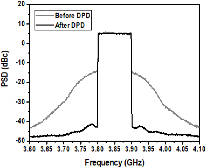
그림 8은 중심주파수 3.85 GHz, 9 dB OBO에서 앞서 사용한 5G NR 신호를 이용하여 측정한 DPD(digital pre-distortion) 기법을 적용하기 전과 후의 스펙트럼이다. DPD 기법 적용 이후 ACLR은 −24 dBc에서 −49 dBc로 개선되었다.
그림 8. | Fig. 8.
5G NR 신호를 이용하여 측정한 DPD 전/후 스펙트럼 | Measured spectrum using the 5G NR signal before and after DPD.
Download Original Figure
표 2에 제안된 DPA의 측정 결과와 OCC나 CCL을 단독으로 적용한 이전의 연구 결과들의 성능비교를 정리하였다. 제안된 전력증폭기가 이전의 연구 결과들과 비교하여 넓은 주파수 대역에서 확장된 OBO를 가진다.
표 2. | Table 2.
이전에 보고된 DPA와 성능 비교 | Performance comparison with the previous works.
| Ref. |
Freq. (GHz) |
Topology |
Psat (dBm) |
DEsat (%) |
OBO (dB) |
DEOBO (%) |
| [8] |
1.68 |
CCL |
43.5 |
73.9 |
9.5 |
56.4 |
| [11] |
3.5~3.6 |
CCL |
42~43 |
60~64.7 |
7~8 |
48~48.5 |
| [16] |
2.1~2.3 |
OCC |
43.6 |
69~71 |
9 |
40~54 |
| [17] |
3.3 |
OCC |
42.3 |
76.9 |
9 |
59.6 |
| This work |
3.7~4.0 |
OCC+CCL |
43.0~44.3 |
72.5~77.9 |
9 |
41.5~48.4 |
Download Excel Table
Ⅳ. 결 론
본 논문에서는 OCC와 CCL을 함께 적용하여 확장된 OBO를 가지는 DPA를 설계하였다. OCC나 CCL을 단독으로 적용할 경우 출력 네트워크의 임피던스들이 각각 하나의 값으로 결정된다. 반면, OCC와 CCL을 함께 적용하면 출력 네트워크의 임피던스들을 선택할 수 있게 되어 회로 설계에 자유도가 생긴다. 제작된 DPA는 3.7~4.0 GHz에서 CW를 이용하여 43.0~44.3 dBm의 출력전력, 8.0~8.5 dB의 gain을 얻었다. Peak power에서 72.5~77.9 %의 DE, 9 dB OBO에서 41.5~48.4 %의 DE를 얻었다. 7.8 dB의 PAPR을 갖는 5G NR 100 MHz 64-QAM OFDM 신호를 이용하여 8.2~8.7 dB의 gain과 9 dB OBO에서 45.6~50.0 %의 DE, −22.0~−26.6 dBc의 ACLR을 얻었다.
Acknowledgements
이 연구는 2023학년도 산업통상자원부 및 산업기술평가관리원(KEIT) 연구비 지원에 의한 연구임(20017971).
References
B. Kim, J. Kim, I. Kim, and J. Cha, "The Doherty power amplifier,"
IEEE Microwave Magazine, vol. 7, no. 5, pp. 42-50, Oct. 2006.


Y. Yang, J. Cha, B. Shin, and B. Kim, "A fully matched N-way Doherty amplifier with optimized linearity,"
IEEE Transactions on Microwave Theory and Techniques, vol. 51, no. 3, pp. 986-993, Mar. 2003.
J. Kim, J. Cha, I. Kim, and B. Kim, "Optimum operation of asymmetrical-cells-based linear Doherty power amplifiers-uneven power drive and power matching,"
IEEE Transactions on Microwave Theory and Techniques, vol. 53, no. 5, pp. 1802-1809, May 2005.
Y. S. Lee, M. W. Lee, and Y. H. Jeong, "Unequal-cells-based GaN HEMT Doherty amplifier with an extended efficiency range,"
IEEE Microwave and Wireless Components Letters, vol. 18, no. 8, pp. 536-538, Aug. 2008.
J. Son, I. Kim, J. Moon, J. Lee, and B. Kim, "A highly efficient asymmetric Doherty power amplifier with a new output combining circuit," in
2011 IEEE International Conference on Microwaves, Communications, Antennas and Electronic Systems(COMCAS 2011), Tel Aviv, Nov. 2011, pp. 1-4.
J. Kim, B. Fehri, S. Boumaiza, and J. Wood, "Power efficiency and linearity enhancement using optimized asymmetrical Doherty power amplifiers,"
IEEE Transactions on Microwave Theory and Techniques, vol. 59, no. 2, pp. 425-434, Feb. 2011.
J. Pang, S. He, Z. Dai, C. Huang, J. Peng, and F. You, "Design of a post-matching asymmetric Doherty power amplifier for broadband applications,"
IEEE Microwave and Wireless Components Letters, vol. 26, no. 1, pp. 52-54, Jan. 2016.
W. Choi, H. Kang, H. Oh, K. C. Hwang, K. Y. Lee, and Y. Yang, "Doherty power amplifier based on asymmetric cells with complex combining load,"
IEEE Transactions on Microwave Theory and Techniques, vol. 69, no. 4, pp. 2336-2344, Apr. 2021.
X. H. Fang, K. K. M. Cheng, "Extension of high-efficiency range of Doherty amplifier by using complex combining load,"
IEEE Transactions on Microwave Theory and Techniques, vol. 62, no. 9, pp. 2038-2047, Sep. 2014.
X. H. Fang, K. K. M. Cheng, "Broadband, wide efficiency range, Doherty amplifier design using frequency-varying complex combining load," in
2015IEEE MTT-S International Microwave Symposium, Phoenix, AZ, May 2015, pp. 1-4.
J. Kim, W. Choi, Y. Choi, H. Oh, and Y. Yang, "3.5 GHz high-efficiency asymmetric Doherty power amplifier design using a complex combining load,"
Journal of Korean Institute of Electromagnetic Engineering and Science, vol. 32, no. 8, pp. 708-716, Aug. 2021.
S. Honda, S. Sakata, Y. Komatsuzaki, and S. Shinjo, "Efficiency enhancement of GaN Doherty power amplifier at large power back-off with virtual short stub technique," in
2019 IEEE Asia-Pacific Microwave Conference (APMC), Singapore, Dec. 2019, pp. 294-296.
K. Horiguchi, S. Ishizaka, T. Okano, M. Nakayama, H. Ryoji, and Y. Isota, et al., "Efficiency enhancement of 250W Doherty power amplifiers using virtual open stub techniques for UHF-band OFDM applications," in
2006IEEE MTT-S International Microwave Symposium Digest, San Francisco, CA, Jun. 2006, pp. 1356-1359.
Y. Chen, W. Choi, J. Shin, H. Jeon, S. Bae, and Y. C. Choi, et al., "Generalized expression and design method of modified load networks for Doherty power amplifier with extended back-off range,"
IEEE Access, vol. 10, pp. 77487-77497, Jul. 2022.
Y. C. Choi, W. Choi, H. Oh, Y. Chen, J. Shin, and H. Jeon, et al., "Doherty power amplifier with extended high-efficiency range based on the utilization of multiple output power back-off parameters,"
IEEE Transactions on Microwave Theory and Techniques, vol. 70, no. 4, pp. 2258-2270, Apr. 2022.
M. R. Hasin, J. Kitchen, "Exploiting phase for extended efficiency range in symmetrical Doherty power amplifiers,"
IEEE Transactions on Microwave Theory and Techniques, vol. 67, no. 8, pp. 3455-3463, Aug. 2019.
H. Jung, H. Oh, Y. Chen, W. Choi, Y. Choi, and S. Woo, et al., "3.3 GHz Doherty power amplifier having a high-efficiency at 9 dB back-off based on outphasing load networks,"
Journal of Korean Institute of Electromagnetic Engineering and Science, vol. 32, no. 11, pp. 971-979, Nov. 2021.