
 PDF Download
 PubReader
 Export Citation
 Email the Author
 Share Facebook
 Share Twitter
 Cited by 0 Article
 Metrics (View:95)









I. Introduction
Recently, highly integrated and high-power electromagnetic systems have increasingly required electromagnetic absorbers to reduce unwanted reflections and mitigate electromagnetic interference (EMI)[1]. In electromagnetic absorbers, the absorbed electromagnetic energy is converted into thermal energy through dielectric, conductive, or resistive losses[2]. In high-power applications such as radar systems, communication platforms, and RF equipment, localized loss concentration can generate severe hotspots, causing variations in material properties and resistance values and degrading absorption performance and long-term reliability[3]. Therefore, for high-power absorber applications, not only the absorption performance but also the heat-dissipation capability should be carefully considered[4].
Resistor-loaded absorbers are widely used for broadband absorption by lowering the resonator quality factor and introducing dissipative loss[5]. However, the localized loss around the resistors can induce hotspots, resulting in a trade-off between absorption bandwidth and thermal reliability[6].
In this paper, a resistor-loaded via-shorted absorber is proposed. The resistor-loaded resonator enables broadband absorption, while the shorting vias provide additional thermal conduction paths from the hotspot region to the ground plane, thereby achieving broadband absorption and hotspot mitigation.
II. Via-shorted Absorber Design
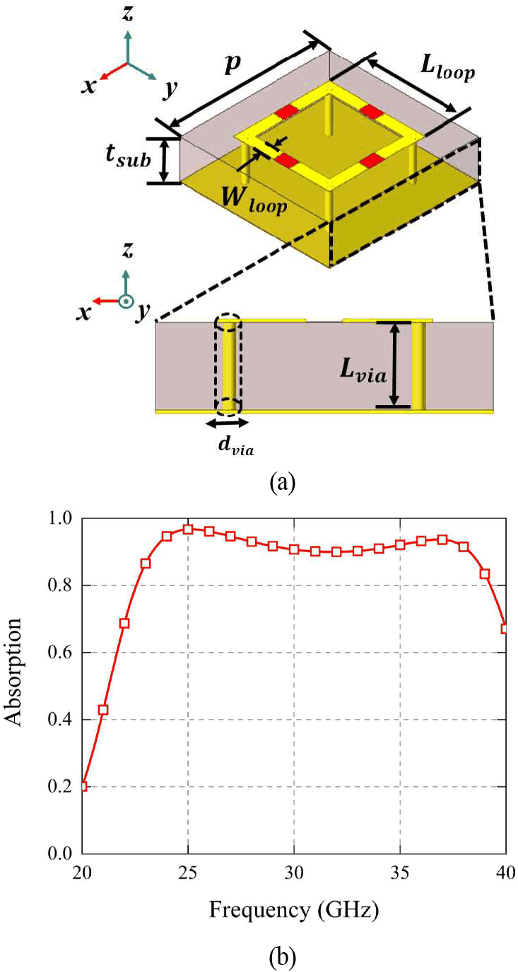
Fig. 1(a) illustrates the proposed via-shorted absorber, which consists of a 1.05 mm-thick FR-4 substrate (εr=4.4 and tan δ=0.02). A resistor-loaded square loop is printed on the top layer and shorting via connect the resonator to the ground to achieve broadband absorption by tuning quality factor and enhancing magnetic resonance. The proposed absorber has a unit cell period (p) of 4.65 mm. The side length of the square loop (Lloop) is set to be 3.2 mm and the line width (Wloop) is 0.36 mm. The via length (Lvia) is 1.05 mm, which is determined by the substrate thickness (tsub), and the via diameter (dvia) is 0.15 mm. In Fig. 1(b), this proposed absorber demonstrates the absorption bandwidth from 23.3 to 38.3 GHz under normal incidence.
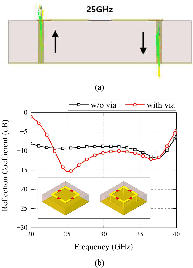
The shorting vias provide additional vertical current paths between the square-loop resonator and the ground plane. As shown in Fig. 2(a), anti-parallel vertical currents flow through adjacent vias, forming a circulating current loop associated with magnetic resonance. This via-induced resonance improves the low-frequency absorption. This results in a broader absorption bandwidth, as demonstrated in Fig. 2(b).
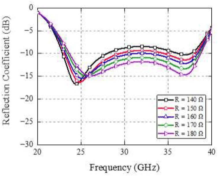
The resistors were located at the current-concentrated regions for dissipative loss, controlling the quality factor of the absorber. In Fig. 3, higher resistance increases the resistive damping and reduce the quality factor of the absorber. However, excessive resistive loading degrades the impedance matching at the resonant frequencies. In contrast, lower resistance increases the quality factor, reducing the absorption bandwidth. Considering theses trade-offs, a resistance of 160 Ω was adopted for maintaining broadband absorption with good impedance matching.
III. Electromagnetic-Thermal Analysis
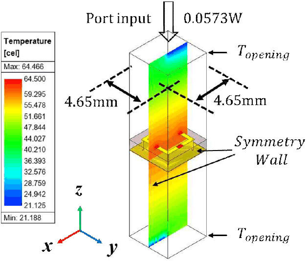
The steady-state temperature distribution of the proposed absorber was analyzed by using ANSYS HFSS and Icepak. In order to compare the heat-spreading effect of the shorting vias, the absorbers with and without shorting vias were simulated under identical absorption power conditions. Each structure was evaluated at a frequency corresponding to 90 % absorption, which ensures identical absorbed-power conditions for the thermal comparison. An input power of 0.0573 W was applied to each unit cell, which is equivalent to an incident electric field strength of 1,000 V/m (2,653 W/m2).
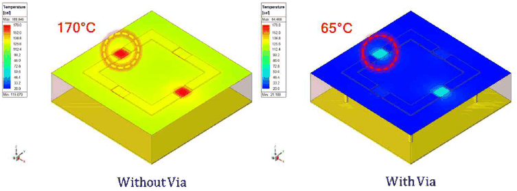
In Fig. 4, the opening boundary was set to an ambient temperature of 20 °C, while symmetry boundary conditions were applied to the lateral sides. Fig. 5 compares the simulated steady-state temperature distributions of the absorber with and without shorting vias. The maximum temperature decreased from 170 °C to 65 °C with the introduction of the shorting vias. A 70 % reduction in the maximum temperature rise was achieved from 150 °C to 45 °C. The resulting maximum temperature of 65 °C is below the reference temperatures of the constituent materials in Table 1. The copper shorting vias provide additional vertical heat-conduction paths from the resistor-loaded resonator to the ground plane, reducing localized heat accumulation around the resistive elements.
| Component | Thermal limit (°C) |
|---|---|
| Standard FR-4[7] | 135 |
| 0402 chip resistor[8] | 155 |
| SAC305 solder joint[9] | 217 |
IV. Conclusion
A via-shorted absorber was proposed to achieve broadband absorption and thermal hotspot mitigation. By integrating a resistor-loaded square-loop resonator with ground-connected shorting vias, this proposed absorber exhibits over 90 % absorption bandwidth from 23.3 to 38.3 GHz. The electromagnetic-thermal analysis demonstrates that the shorting vias reduced the hotspot temperature from 170 °C to 65 °C, corresponding to a 70 % reduction in maximum temperature rise. Future work will focus on the fabrication and experimental characterization of the proposed absorber to validate its broadband absorption and thermal hotspot mitigation effect. This proposed via-shorted configuration can provide an effective approach for improving hotspot mitigation while maintaining broadband absorption.


