단편논문/SHORT PAPERS
6G Upper-Mid Band 이동통신용 고출력 CMOS 1채널 빔포밍 송신단
오의진†
,
조은채†,
이민규†,
모은수,
왕승훈,
이희동,
박봉혁,
이승찬†,
박진석
High-Power CMOS 1-Channel Beamforming Transmitter for 6G Upper-Mid Band Communications
Eui-Jin Oh†,
Eun-Chae Jo†,
Min-Gyu Lee†,
Eun-Su Mo,
Seung-hun Wang,
Hui-Dong Lee,
Bong-Hyuk Park,
SeungChan Lee†,
Jinseok Park
Author Information & Copyright ▼
Department of Intelligent Electronics and Computer Engineering, Chonnam National University
Department of Electronic Engineering, Chonnam National University
Electronics and Telecommunications Research Institute
† These authors contributed equally to this work.
© Copyright 2025 The Korean Institute of Electromagnetic Engineering and Science. This is an Open-Access article distributed under the terms of the
Creative Commons Attribution Non-Commercial License (http://creativecommons.org/licenses/by-nc/4.0/) which permits
unrestricted non-commercial use, distribution, and reproduction in any
medium, provided the original work is properly cited.
Received: Jun 17, 2025; Revised: Jul 10, 2025; Accepted: Aug 18, 2025
Published Online: Aug 31, 2025
요 약
본 논문에서는 6G upper-mid band에서 동작하는 CMOS 1채널 빔포밍 front-end IC를 설계하였다. 설계한 1채널 빔포밍 칩은 이득과 위상 조절을 위한 가변 이득 위상천이기와 높은 출력 전력을 위한 전력증폭기로 구성된다. 가변 이득 위상천이기는 IQ 생성기, 이득 조절을 위한 2개의 벡터 생성기, 그리고 벡터 합 회로로 구성된다. 전력증폭기는 높은 선형 출력 전력을 위해 Cold-Fet 기반의 선형화기를 drive stage에 사용하였다. 제안하는 1채널 빔포밍 칩은 15.1 GHz에서 이득 26.8 dB, P1dB 23 dBm, RMS phase error 0.8°, AM-AM distortion 0.9 dB, AM-PM distortion 1.7°, 3 dB 대역폭은 14.1~18.2 GHz를 갖는다. 제안된 1채널 전치단 회로는 65-nm CMOS 공정을 사용하여 제작되었으며, 패드를 제외한 칩의 크기는 0.79 mm2이다.
Abstract
This study presents a CMOS 1-channel beamforming front-end IC for 6G upper midband communications. The proposed chip consists of a variable gain phase shifter (VGPS) for gain and phase control and a power amplifier (PA) for high output power. The VGPS consists of an IQ generator, two vector generators, and a vector-summing circuit. The chip is fabricated using a 65-nm CMOS process, and its core area, excluding the pads, was 0.79 mm². To achieve a high linear output power, a cold-FET-based linearizer is implemented in the drive stage. The proposed 1-channel beamforming chip achieved a gain of 26.8 dB, P1dB of 23 dBm, rms phase error of 0.8°, AM-AM distortion of 0.9 dB, and AM-PM distortion of 1.7° at 15.1 GHz. The 3 dB bandwidth ranges from 14.1 to 18.2 GHz.
Keywords: 6G Upper-Mid Band; Beamforming; Power Amplifier; Phase Shifter; Variable Gain
Ⅰ. 서 론
차세대 6G 통신은 초고속 데이터 전송, 초저지연, 초연결성을 목표로 하며 이를 위해 다양한 주파수 대역이 연구되고 있다. 특히 upper-mid band 대역은 기존 5G 주파수보다 높은 성능을 제공하면서도 밀리미터파(mmWave) 대역보다는 전파 손실이 적어 차세대 통신 주파수로서 큰 주목을 받고 있다. 6G upper-mid Band 대역의 후보 주파수는 세계전파통신회의(WRC-23) 회의에서 4.4~4.8 GHz, 7.125~8.5 GHz, 14.8~15.35 GHz 3가지로 고려됐다[1]. 본 논문에서는 동일한 면적 내에서 훨씬 더 많은 안테나를 집적할 수 있고, 높은 전송속도를 확보할 수 있는 15 GHz 대역의 회로를 개발하였다.
Upper-mid band 대역의 6G 통신에서는 경로 손실을 보상하고 전력 효율성을 극대화할 수 있는 빔포밍(beamforming) 기술이 필수적이다. 빔포밍 시스템을 구현하기 위해서는 다채널 빔포밍 IC가 필요하고, 채널의 수가 많아질수록 필요한 PA의 개수도 증가한다. CMOS 기반의 PA는 집적도가 높기 때문에, 빔포밍 시스템을 구현하기에 매우 적합하다. 하지만, 기존의 CMOS PA는 출력 전력이 낮아 고출력을 위한 화합물 PA나 combined PA가 추가로 필요하다. 하지만, 화합물 PA를 사용하는 경우 모듈의 사이즈와 가격이 크게 증가하고, combined PA를 사용하는 경우 높은 복잡도와 큰 사이즈로 다채널 빔포밍 IC에 집적하기 어렵다. 따라서 본 논문에서는 빔포밍 시스템을 위한 고출력 전력 증폭기와 가변 이득 위상천이기를 집적한 송신 1채널을 제안하고 있으며, 1-way 구조이지만 Combined PA만큼 높은 출력 전력과 낮은 RMS phase error를 확보하여 6G 통신 환경에서의 빔포밍 성능을 향상시키고자 한다.
Ⅱ. 1채널 빔포밍 Front-End IC 설계
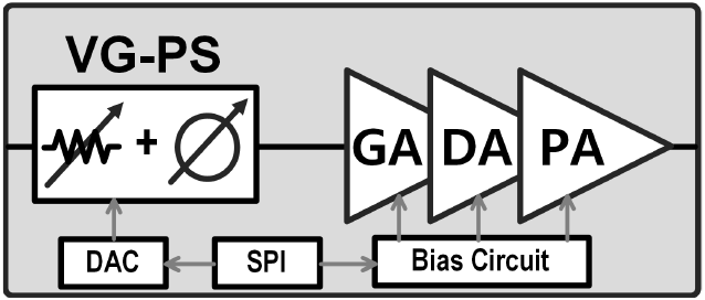
그림 1은 본 논문에서 제안하는 1채널 빔포밍 송신단의 구성도이다. 이득과 위상 조절을 위한 가변 이득 위상천이기와 고출력을 위한 3 stage PA로 구성된다.
2-1 전력증폭기 구조
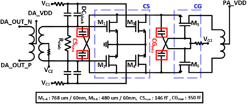
그림 2는 제안하는 PA의 power stage의 회로도이다. power stage는 cascode 구조로 설계하였고, common source (CS) 증폭기는 시스템이 요구하는 높은 선형 출력을 확보하기 위해 MGTR(multi-gate transistor) 구조로 설계하였으며, 동작 안정성을 높이기 위해 CS neutralized 커패시터를 사용하였다. 또한 CG cross coupled cap을 사용해 높은 S(2,2)를 확보하였다. CS 전력증폭기에 0.6 V의 높은 bias를 사용하면 큰 파워 영역에서 gain compression이 일어나고, 0.3 V의 낮은 bias를 사용하면 gain expansion이 일어난다. MGTR CS 증폭기의 각 트랜지스터에 각각 0.3 V, 0.6 V 전압을 공급함으로써 이러한 상보적인 특징을 이용하여 일반적인 CS 증폭기 대비 P1 dB를 1 dB 개선하였다.
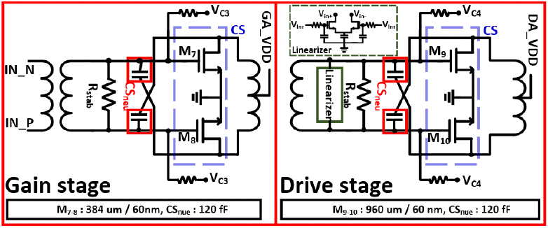
그림 3은 제안하는 PA의 gain, drive stage의 회로도이다. 각 Stage는 모두 CS 증폭기 구조로 설계하였으며 power stage와 마찬가지로 동작 안정성을 높이기 위해 CS neutralized 커패시터를 사용하였다. 또한 높은 선형 출력을 위해 drive stage에 Cold-Fet 기반의 선형화기를 사용했다[2].
그림 3. | Fig. 3.
제안하는 전력증폭기의 gain, drive stage 회로도 | Schematics of gain and drive stage amplifier.
Download Original Figure
2-2 가변 이득 위상천이기 구조
본 논문에서 설계한 가변 이득 위상천이기는 vector 생성기, IQ 신호 생성기, 위상과 이득을 제어하는 DAC, 그리고 사분면 스위치로 구성된다[3]. IQ 생성기는 RC-RL 구조를 통해 vector 생성기와 IQ 생성기 사이의 임피던스 불균형을 해결하고 낮은 삽입손실을 확보하였다[4]. 또한 Gilbert cell 구조의 vector 생성기는 위상 및 이득 state에 상관 없이 총 전류가 일정하게 유지되도록 설계하였다[5],[6]. 이를 통해 위상과 이득이 바뀌더라도 출력 임피던스가 유지되어 이득 및 위상 조절에 따른 위상 오차가 개선되었다.
Ⅲ. 실험 및 측정 결과
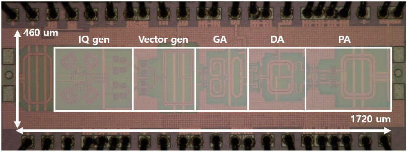
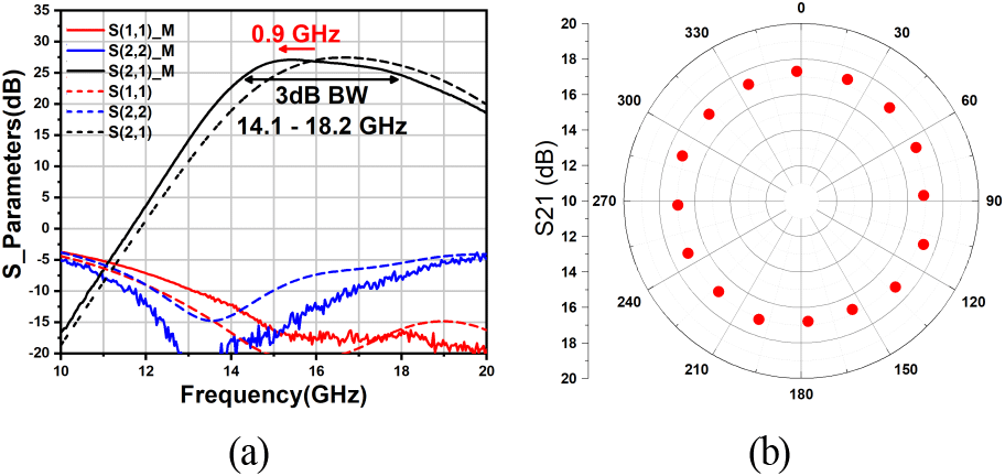
본 논문에서 제안하는 1채널 빔포밍 송신단은 65 nm CMOS 공정으로 제작하였다. 그림 4는 제작된 1채널 송신단 칩의 칩 사진이다. 패드를 제외한 칩의 크기는 0.79 mm2이다. 전체 소비전력은 696 mW이며, 각각 PA 634 mW, DA 7 mW, GA 45 mW, PS 10 mW이다. 그림 5는 S-parameters 측정 결과와 15 GHz에서 측정한 1채널 빔포밍 IC의 성상도이다. 15.1 GHz에서 26.8 dB의 이득을 가지며, 3dB 대역폭은 14.1~18.2 GHz이다. 성상도는 고분해능 위상천이기를 이용해 오차가 캘리브레이션 되었으며, 이를 통해 얻은 RMS 위상 오차는 0.8°이다. 이득 조절에 따른 peak-to-peak 위상 오차는 1.9°, PAE는 33 %이며, 이는 시뮬레이션 결과이다.
그림 4. | Fig. 4.
제안하는 1채널 빔포밍 front-end IC 칩 사진 | Proposed 1-channel beamforming front-end ic chip photograph.
Download Original Figure
그림 5. | Fig. 5.
(a) S-parameters 측정결과 (b) 15 GHz에서 측정한 1채널 빔포밍 IC의 성상도 | (a) Measured results of the S-parameters (b) Measured static vector Constellation of 1-channel beamforming IC at 15 GHz.
Download Original Figure
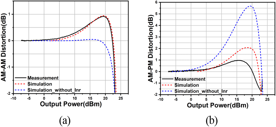
그림 6은 15 GHz에서 측정한 AM-AM Distortion과 AM-PM Distortion이다. 각각 0.9 dB, 1.7°도 이고 P1 dB는 23 dBm이다. 표 1은 본 논문이 제안하는 1채널의 성능 요약 및 PA reference들과의 성능 비교표이다. 본 논문이 제안하는 1채널 송신단은 2-way combine PA만큼 높은 출력 전력을 갖으며, 가장 낮은수준의 RMS 위상 오차를 갖는다.
그림 6. | Fig. 6.
15 GHz에서 측정한 (a) AM-AM 왜곡, (b) AM-PM 왜곡 | Measured (a) AM-AM distortion and (b) AM-PM distortion at 15 GHz.
Download Original Figure
표 1. | Table 1.
성능 요약 및 비교표 | Performance summary and comparison table.
| Ref. |
This work |
[7]
|
[8]
|
[9]
|
[10]
|
| Tech |
65 nm CMOS |
65 nm CMOS |
65 nm CMOS |
65 nm CMOS |
28 nm CMOS |
| Architecture |
1-way |
2-way combine |
1-way |
1-way |
1-way |
| Freq (GHz) |
15 |
13~15 |
10 |
28~30 |
60 |
| 3 dB BW (GHz) |
14.1~18.2 |
12.3~15.6 |
- |
- |
57~63.3 |
| Supply (V) |
2..2 |
1/2.2 |
1/1.8 |
1.8 |
- |
| Peak gain (dB) |
24 |
26~27.3 |
- |
25.6 |
20 |
| OP1 dB (dBm) |
23 |
22.7~22.9 |
21 |
15 |
10.8 |
| RMS phase error (degree) |
0.8 |
- |
- |
2.7 |
2.76 |
Download Excel Table
Ⅳ. 결 론
본 논문은 upper-mid 대역에서 동작하는 1채널 빔포밍 송신단 IC를 제안하였다. 3 stage PA를 통해 높은 출력 전력과 이득을 확보하였으며, 선형화기를 사용해 높은 선형 출력 전력을 확보하였다. 또한 RC-RL 구조의 IQ 생성기와 Gilbert cell 구조의 벡터 생성기로 이루어진 가변 이득 위상천이기를 통해 낮은 RMS 위상 오차를 달성하였다.
Acknowledgements
「이 성과는 정부(과학기술정보통신부)의 재원으로 한국 연구재단의 지원을 받아 수행된 연구임(RS-2023-00211916).」
「본 연구는 IDEC에서 EDA Tool을 지원받아 수행하였습니다.」
「이 논문은 정부(과학기술정보통신부)의 재원으로 정보통신기획평가원–학·석사연계ICT핵심인재양성 지원을 받아 수행된 연구임(IITP-2025-RS-2024-00436837).」
References
World Radiocommunication Conference 2023(WRC-23) Final Acts, ITU-R, Dec. 2023.

J. Lim, W. Lee, S. M. Moon, E. Oh, S. Wang, and D. Chang, "A K-Band CMOS power amplifier using an analog predistortion linearizer with 22.1 dBm psat and 0.9° AM-PM distortion," in
2024 IEEE Radio Frequency Integrated Circuits Symposium(RFIC), Washington, DC, Jun. 2024, pp. 303-306.

M. G. Lee, S. B. Lim, G. H. Jeong, J. S. Park, and S. C. Hong, "A Ka-Band variable gain phase shifter with a non-linear DAC,"
The Journal of Korean Institute of Electromagnetic Engineering and Science, vol. 34, no. 11, pp. 844-847, Nov. 2023.
S. Wang, J. Park, and S. Hong, "A K-Band variable-gain phase shifter based on Gilbert-Cell vector synthesizer with RC–RL poly-phase filter,"
IEEE Microwave and Wireless Components Letters, vol. 31, no. 4, pp. 393-396, Apr. 2021.
J. Park, S. Lee, J. Chun, L. Jeon, and S. Hong, "A 28-GHz four-channel beamforming front-end IC with dual-vector variable gain phase shifters for 64-element phased array antenna module,"
IEEE Journal of Solid-State Circuits, vol. 58, no. 4, pp. 1142-1159, Apr. 2023.
J. Park, S. Lee, D. Lee, and S. Hong, "9.8 A 28GHz 20.3%-transmitter-efficiency 1.5°-phase-error beamforming front-end IC with embedded switches and dual-vector variable-gain phase shiftesrs," in
2019 IEEE International Solid-State Circuits Conference(ISSCC), San Francisco, CA, Feb. 2019, pp. 176-178.
J. H. Kim, J. T. Lim, J. E. Lee, J. H. Song, J. T. Son, and M. S. Baek, "An efficient Ku-band two-way vertical-like power-combining power amplifier using merged inter-stage transformers achieving 23-23.4 dBm psat and 45.2-46.6% peak PAE in 65nm CMOS," in
2024 IEEE Radio Frequency Integrated Circuits Symposium(RFIC), Washington, DC, Jun. 2024, pp. 299-302.
J. Li, R. Shu, Z. Xu, and Q. J. Gu, "A 21-dm-OP
1dB 20.3%-Efficiency−131.8-dBm/Hz-Noise X-band cartesian error feedback transmitter with fully integrated power amplifier in 65-nm CMOS," in
IEEE Journal of Solid-State Circuits, vol. 55, no. 6, pp. 1491-1501, Jun. 2020.
T. Huang, X. Meng, C. Chen, G. Zhao, P. Bai, and Y. Yin, "A Ka-Band transmitter with 2.7°/0.28 dB phase/gain error and 21.6% PAE maintaining stable performance across process corners,"
IEEE Transactions on Microwave Theory and Techniques, no. 99, pp. 1-11, Apr. 2024.
C. So, E. T. Sung, and S. Hong, "A V-band four-channel phased array transmitter beamforming IC with 0.7-degree phase step in 20 dB dynamic range," in
2023 IEEE Radio Frequency Integrated Circuits Symposium(RFIC), San Diego, CA, Jul. 2023, pp. 41-44.