논문/REGULAR PAPERS

위성 Synthetic-Aperture Radar (SAR) 시스템용 X-밴드 이중 편파 마이크로스트립 패치 부배열 안테나

크리스티얀디미트로브1https://orcid.org/0000-0001-5153-9610, 이용식1,https://orcid.org/0000-0003-2623-3569, 윤성식*https://orcid.org/0000-0002-5764-5403, 조승주*https://orcid.org/0000-0001-8999-6796, 송찬미*https://orcid.org/0000-0003-1723-3006, 송성찬*https://orcid.org/0000-0003-0965-2091
Kristian Dimitrov1https://orcid.org/0000-0001-5153-9610, Yongshik Lee1,https://orcid.org/0000-0003-2623-3569, Seongsik Yoon*https://orcid.org/0000-0002-5764-5403, Seung Joo Jo*https://orcid.org/0000-0001-8999-6796, Chan Mi Song*https://orcid.org/0000-0003-1723-3006, Sungchan Song*https://orcid.org/0000-0003-0965-2091
Author Information & Copyright
1연세대학교 전기전자공학과
*한화시스템 항공·우주연구소
1Department of Electrical and Electronic Engineering, Yonsei University
*Aerospace R&D Center, Hanwha Systems
Corresponding Author: Yongshik Lee (e-mail: yongshik.lee@yonsei.ac.kr)

© Copyright 2021 The Korean Institute of Electromagnetic Engineering and Science. This is an Open-Access article distributed under the terms of the Creative Commons Attribution Non-Commercial License (http://creativecommons.org/licenses/by-nc/4.0/) which permits unrestricted non-commercial use, distribution, and reproduction in any medium, provided the original work is properly cited.

Received: Aug 26, 2021; Revised: Sep 07, 2021; Accepted: Dec 08, 2021

Published Online: Dec 31, 2021

요약

본 연구에서는 위성 SAR 시스템용 이중 편파 패치 안테나를 제안한다. 안테나는 스트립라인 급전 회로로부터 개구면을 통해서 급전된 적층형 패치로, 급전 네트워크 사이에 높은 격리도와 광대역 특성을 제공한다. 또한, 스트립라인-슬롯 전환에 의해 여기된 병렬 플레이트 모드를 억제하여 효율을 증가시켰다. 설계된 안테나는 Taconic의 고성능 저손실 RF-35 기판과 함께 안테나의 반사 특성 대역폭을 극대화하고 손실을 최소화하기 위해 허니콤 구조를 적층시킨 유전체를 사용하여 2×4 배열로 설계, 제작하였다. 측정 결과, 안테나의 최대 이득은 15.7 dBi이며, 40 dB 이상의 높은 교차 편파 분리도 (Cross-polarization Discrimination, XpD)와 19.4 % 이상의 넓은 −10 dB 반사 대역폭 등 우수한 성능을 나타내었다.

Abstract

In this study, a high-performance, dual linearly polarized patch array antenna is presented for satellite synthetic aperture radar (SAR) applications. The antenna features an aperture-fed stacked patch as the radiation element and a stripline feeding network. A high-performance and low-loss dielectric substrate RF-35 by Taconic, and a honeycomb substrate is used. The honeycomb substrate is used to maximize the impedance bandwidth and decrease the insertion loss of the antenna. The proposed antenna offers exceptional isolation between the antenna’s ports in excess of 55 dB owing to its stripline feeding network. The via stitching technique is utilized to suppress the parallel-plate mode excited by the discontinuities in the stripline. The antenna is designed to possess a wide impedance bandwidth. A prototype antenna of size 2×4 elements, which operates in the X-band, is fabricated. Its impedance and radiation performance are experimentally verified, and the results are presented. The antenna exhibits a 15.7 dB peak gain and more than 40 dB of cross-polarization discrimination. In addition, a wide bandwidth of 19.4 % at a −10 dB return loss (RL) level is obtained.

Keywords: SAR; Patch Antenna; Array Antenna; Subarray; X-Band

Ⅰ. INTRODUCTION

Satellite Synthetic-Aperture Radar(SAR) systems require high-performance antennas for optimal operation. Additional weight and profile restrictions to antennas exist in addition to those comparable terrestrial or airborne radar/SAR systems. Microstrip patch arrays have exceptionally low profiles and weights relative to their waveguide or reflector antenna counterparts, making them attractive platforms for spaceborne SAR antennas; they have been recently used extensively in the industry[1][3]. Both single- and dual-polarization antennas have been used in SAR systems. The dual polarization system has an advantage over the standard single polarization antenna, in that it can obtain polarimetric data, thus increasing the pool of information that can be extracted from the target[4].

In this work, a dual linearly polarized microstrip patch array is presented. The antenna has 2×4 radiation elements and operates in X-band, with the center frequency denoted as f0. The antenna is designed to have an impedance bandwidth of more than 12.2% and maximize the gain, with predetermined subarray size of 88.0×44.0 mm2. The antenna is intended to be used as a subarray module in a large-scale array for SAR application. The antenna’s total size is 23×23 wavelengths (at the center frequency f0) in size and has estimated gain of more than 35 dBi. A large array based on a small subarray reduces the overall complexity of the antenna, facilitates larger antenna gain, and allows for beam scanning.

Two independent stripline corporate feeding networks located on the same layer are used to distribute power to the dual-polarization radiation elements. The feeding network simultaneously has inherent wideband performance, excellent polarization isolation and low spurious radiation. It also features only 0.6 dB of simulated insertion loss. However, via stitching, it is necessary to suppress the excitation and propagation of parallel plate modes, due to discontinuities in the feeding network. Using an aperture-fed stacked-patch[5],[6] as the radiation element and a relatively thick honeycomb substrate, a wide impedance bandwidth, in excess of 19 % at Return Loss (RL) level < −10 dB, is obtained. The peak realized gain of the subarray is measured as 15.7 dBi, and the XpD is more than 40 dB.

Ⅱ. ANTENNA DESIGN

Multiple different techniques exist for impedance bandwidth improvement in microstrip patch antennas. Some of them include utilizing thick low-permittivity substrates, multiple coupled resonant elements, co-planar parasitic elements, reactive loading, or variously shaped slots cut in the microstrip patch element. In this study, a coupled stacked patch configuration separated by a thick low-permittivity honeycomb substrate is used. Using this combination, a very wide impedance bandwidth can be obtained. The large separation between the patches ensures low-coupling coefficient between the two patch elements, resulting in closely spaced resonant peaks in the input impedance of the structure.

A small H-shaped modified aperture[7] located in the groundplane separating the feeding network and lower patch element is used to couple power to the radiation elements. The substrate used between the lower patch and coupling aperture is relatively thin and has high permittivity; thus, a high coupling coefficient can be achieved for a relatively small aperture size. Small apertures have extremely reactive impedance and do not contribute to radiation. The aperture functions as a step-down transformer, transforming the high input impedance of the patch antenna down to an impedance comparable to that of the transmission lines used in the feeding network.

The designed 2×4 microstrip array is constructed of five dielectric and five conductive layers. The stripline feeding network of two Taconic RF-35[8] dielectric laminate substrates surrounded by two ground planes. The substrate has a nominal dielectric constant of 3.5 and a loss tangent of 0.0018. Similarly, the two radiation patch elements are made on the RF-35 substrate; however, they are separated by an Ultracor UQF-105-1/4[9] honeycomb dielectric layer. This honeycomb material exhibits a dielectric constant near unity, and has an extremely low dielectric loss factor of less than 0.00083. The honeycomb substrate enables wideband impedance performance and the minimization of dielectric loss in the antenna. Additionally, the use of a honeycomb substrate, instead of standard solid dielectric materials, allows for a significantly lower antenna weight[10],[11]. The antenna’s PCB stack-up adopted in this study is shown in Fig. 1.

jkiees-32-12-1031-g1
그림 1. | Fig. 1. 기판 적층 구조 | PCB stack-up.
Download Original Figure

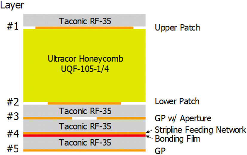
Blind via holes are used to stitch layers #3 and #5, which are the ground planes forming the stripline feeding network. This is done to provide excellent shielding between the two feeding networks, and suppress the excitation of the parallel plate mode by discontinues in the stripline[12],[13].

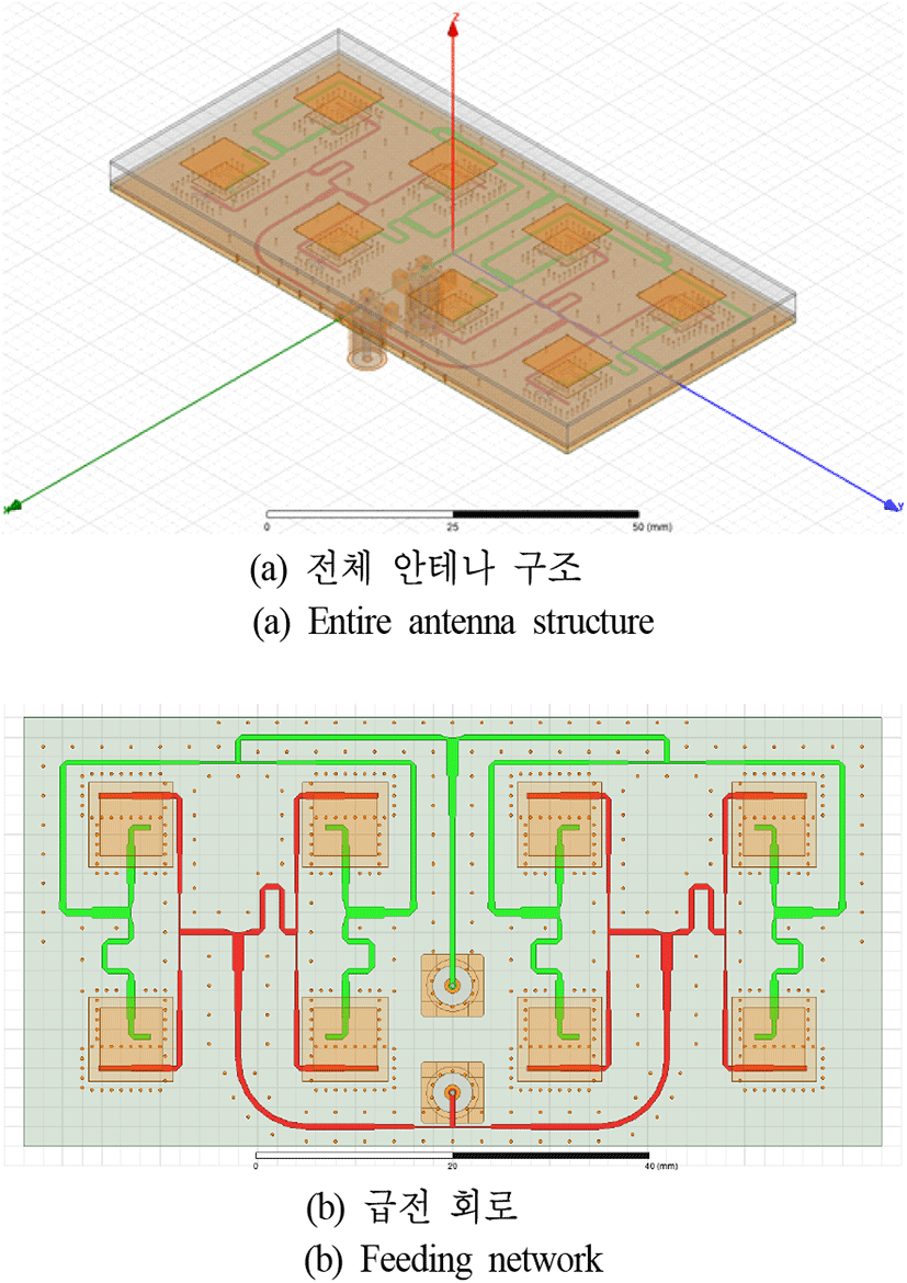
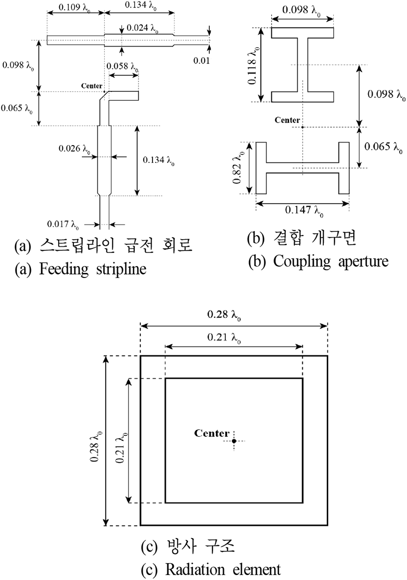
The antenna is designed, and its performance is verified using a commercial electro-magnetic simulator ANSYS HFSS. The simulation model used is shown in Fig. 2. The feeding networks are color-coded as green representing the feeding network facilitating vertically polarized radiation, and red for that of horizontally polarized radiation. The detailed normalized dimensions of the radiation element unit cell are shown in Fig. 3.

jkiees-32-12-1031-g2
그림 2. | Fig. 2. HFSS 시뮬레이션 CAD 모델 | HFSS simulation CAD model.
Download Original Figure
jkiees-32-12-1031-g3
그림 3. | Fig. 3. 방사체의 전류 분포 | Radiation element current distribution.
Download Original Figure

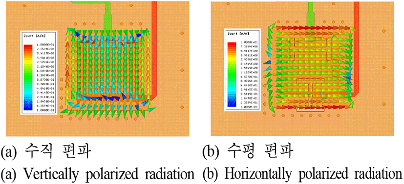
The radiation elements are fed via two orthogonally located apertures placed directly under the radiation elements. Each aperture is fed by the H- or V-pol feeding network. Any coupling between the closely spaced apertures results in an out-of-phase summation within the feeding network of the opposing polarization, resulting in very high isolation between the two polarizations. Fig. 4 shows the current distribution J, on the upper patch of the assembly when only one of the feeding networks is excited.

jkiees-32-12-1031-g4
그림 4. | Fig. 4. 설계 파라미터 (중심 주파수에서 파장 λ0으로 정규화) | Design parameters normalized to wavelength λ0 at center frequency.
Download Original Figure

Ⅲ. SIMULATION AND MEASUREMENT RESULTS

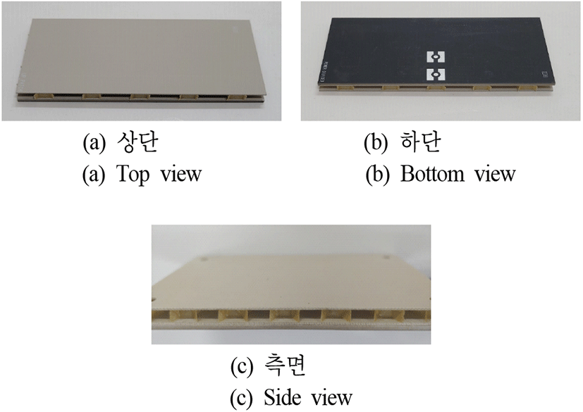
The antenna is fabricated via a standard PCB manufacturing process. The total size of the PCB assembly is 88.0× 44.0×5.1 mm3. Two surface mount SMA-F connectors are used to feed the antenna. The antenna’s RL and isolation are measured using a two-port Anritsu 37247D 20 GHz Vector Network Analyzer (VNA). The radiation pattern and gain of the antenna are measured using a tapered anechoic chamber, MTG antenna measurement system and Agilent Technologies E8364B 50 GHz VNA. Images of the fabricated antenna are shown in Fig. 5.

jkiees-32-12-1031-g5
그림 5. | Fig. 5. 제작된 2×4 마이크로스트립 패치 부배열 안테나 | Fabricated 2×4 patch subarray antenna.
Download Original Figure

A comparison between the measured and simulated RL of the antenna is presented in Fig. 6. The antenna features measured −10 dB RL bandwidth for H- and V-pol of 19.4 % and 21.1 % respectively. Slight frequency shift in the measured impedance bandwidth relative to the simulated RL can be observed. The frequency shift can be caused by the change in the electrical length of components in the feeding network, because of variations in the dielectric constant of the substrate[8]. Moreover, the center frequency of patch antennas is very sensitive to substrate height variations. Bonding film is used to attach the feeding network and stacked patch assemblies, causing significant enough change in height, enough to offset the center frequency. Additionally, the coupling between the two antenna ports is measured as less than −55 dB within the band of interest.

jkiees-32-12-1031-g6
그림 6. | Fig. 6. 부배열 안테나 반사 | Array antenna.
Download Original Figure

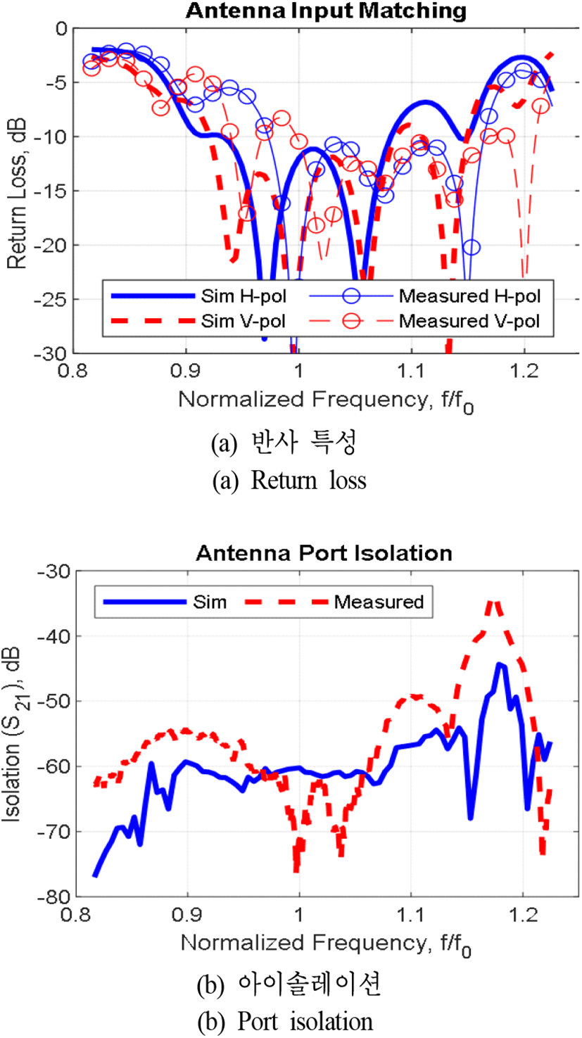
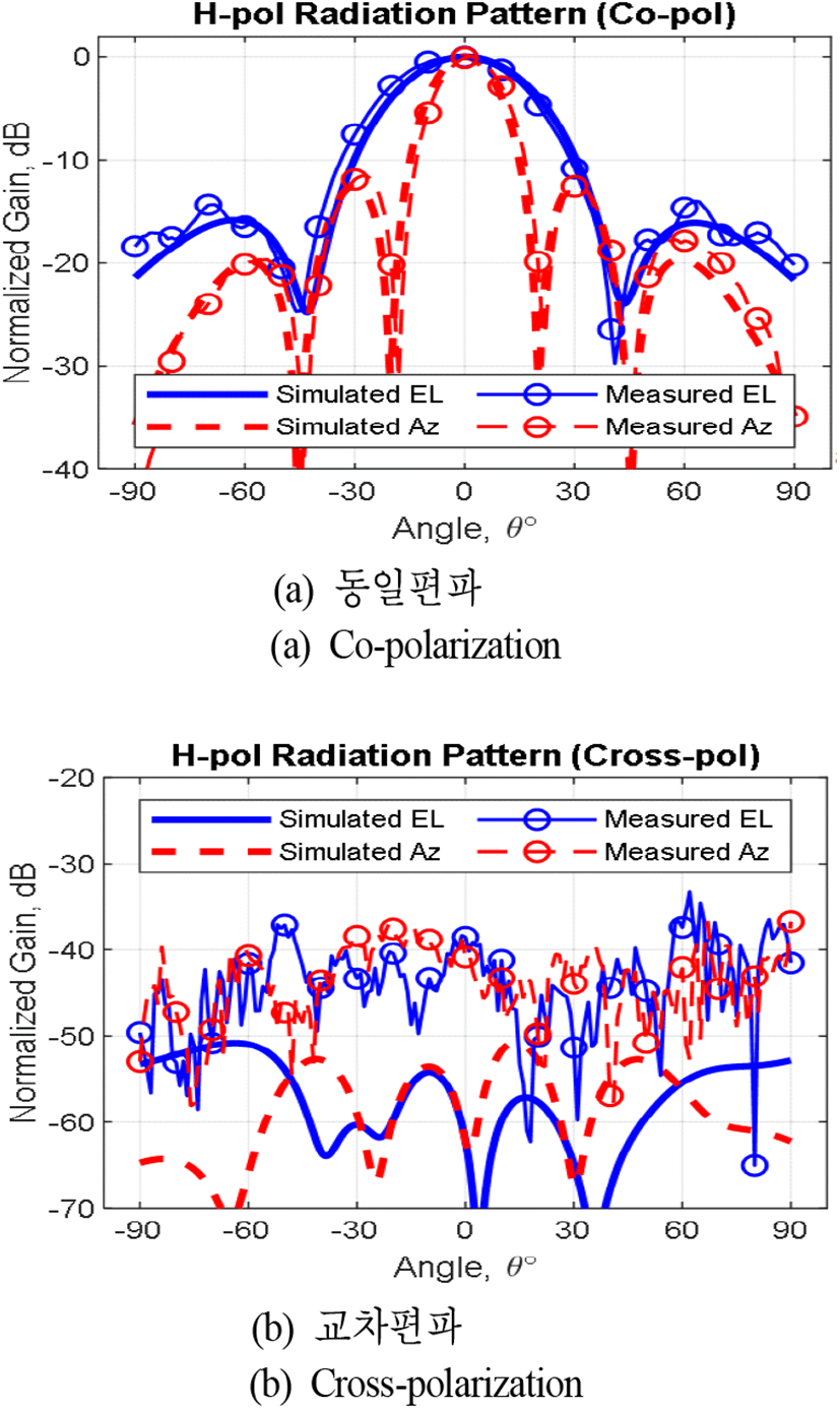
Fig. 7 and Fig. 8 show a comparison of the simulated and measured radiation patterns. Good agreement between the datasets is observed. Respective antenna beam widths of 41°/19° in the elevation and azimuth planes are measured for V-pol radiation, and 37°/18° for H-pol radiation. The obtained Side Lobe Level (SLL) is −12.3 dB for V-pol and −12.6 dB for H-pol. The non-ideal amplitude distribution and mutual coupling between elements causes the SLL to be higher than the ideal value of −13.3 dB.

jkiees-32-12-1031-g7
그림 7. | Fig. 7. 2×4 마이크로스트립 패치 부배열 안테나 수직 편파 방사 패턴 | Horizontal polarization normalized radiation pattern of the 2×4 subarray at the center frequency f0.
Download Original Figure
jkiees-32-12-1031-g8
그림 8. | Fig. 8. 2×4 마이크로스트립 패치 부배열 안테나 수평 편파 방사 패턴 | Vertical polarization normalized radiation pattern of the 2×4 subarray at the center frequency f0.
Download Original Figure

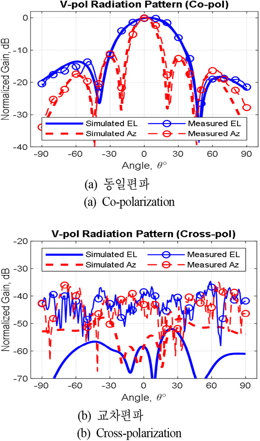
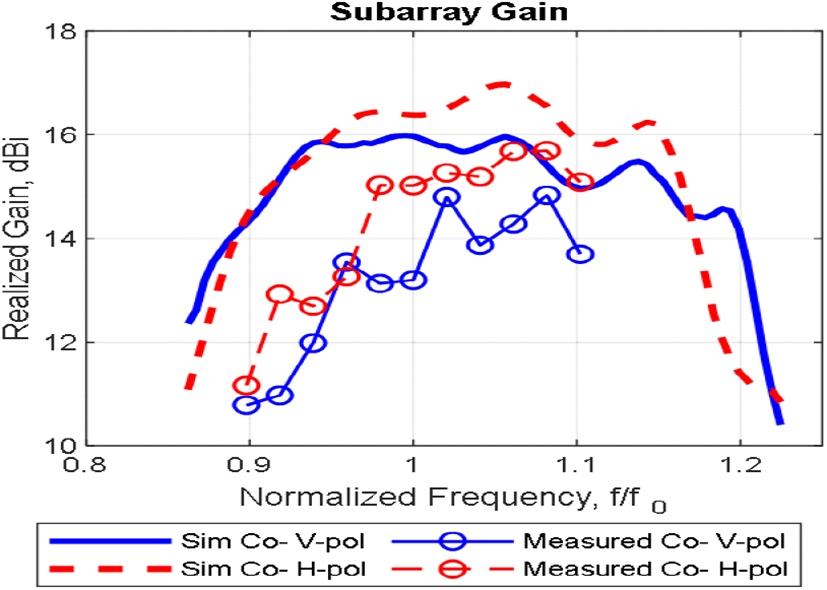
The peak measured gain for H-pol is 15.7 dBi, and that for V-pol 14.8 dBi, as shown in Fig. 9. The measured XpD level is 40 dB for both polarizations, where the simulated value is less than 55 dB. The XpD measurement is limited by the noise performance of the measurement system. Owing to the small dynamic range of the system the measured value of XpD corresponds to the noise floor of the VNA.

jkiees-32-12-1031-g9
그림 9. | Fig. 9. 주파수에 따른 배열 이득 | Subarray gain versus frequency.
Download Original Figure

The performance of the proposed antenna is compared with two other works for SAR applications that utilize microstrip patch as the radiation element. A parameter-wise comparison between the antennas is presented in Table 1. The proposed design exhibits a significantly larger −10 dB impedance bandwidth compared with the other two works. Because [14] does not utilize any parasitic elements in the antenna design, the bandwidth is extremely limited. The largest reported impedance bandwidth in [13] is 11.8 % at RL level of −14 dB, and in [14] of 3 % at −18 dB RL level. It can be seen from [13] and [14] that the −10 dB bandwidth is in the range of only 13 % and 7.1% respectively, compared to the proposed 21.1%. The proposed antenna has significantly higher isolation and XpD than the other two works. This is mainly due to the use of stripline in the feeding network. The via stitching around the stripline limits the coupling between the two polarizations and improves both the isolation and Cross-Polarization Discrimination (XpD) performance of the antenna. The SLL level between the proposed antenna and [13] differs significantly. In this work, the array is uniformly excited, whereas in [13], aperture taper is applied reducing the SLL level and gain.

표 1. | Table 1. 마이크로스트립 패치 배열의 성능 비교 | Comparison of microstrip patch arrays antennas’ performance.
This work Ref. [13] Ref. [14]
Array size 2×4 1×8 1×16
Frequency band X-band X-band X-band
Polarization Dual LP Dual LP Dual LP
Feed type Corporate stripline Corporate microstrip Corporate microstrip
Antenna type Stacked patch Stacked patch Cavity backed patch
RL V-pol 19.4 % @ −10 dB
21.1 % @ −10 dB
8.7 % @ −14dB
11.8 % @ −14 dB
3.0 % @ −18 dB
3.0 % @ −18 dB
H-pol
Max gain V-pol 14.8 dBi
15.7 dBi
13.0 dBi
13.5 dBi
∼21.0 dBi
∼21.0 dBi
H-pol
Isolation > 55 dB > 40 dB > 22 dB
XpD > 40 dB ~ 30 dB > 25 dB
SLL −12.3 dB −20 dB −13.7 dB
Download Excel Table

Ⅳ. CONCLUSION

In this work, a 2×4 element dual linearly polarized stacked patch antenna array is presented. A stripline feeding network is used to provide excellent cross-polarization performance and isolation between the two polarizations. An antenna prototype is manufactured and its impedance and radiation performance are quantified. A wide impedance bandwidth of 21.1 % at an RL level of −10 dB. The antenna exhibits 15.7 dBi gain, XpD in excess of 40 dB and SLL of less than −12.3 dB.

Acknowledgements

이 논문은 2020년도 한화시스템(주)의 재원을 지원받아 수행된 연구임.

References

[1].

X. Zhao, B. N. Tian, S. P. Yeo, and L. C. Ong, “Low-profile broadband dual-polarized integrated patch subarray for X-band synthetic aperture radar payload on small satellite,” IEEE Antennas and Wireless Propagation Letters, vol. 16, pp. 1735-1738, 2017.

[2].

K. Li, T. Dong, and Z. Xia, “A broadband shared-aperture L/S/X-band dual-polarized antenna for SAR applications,” IEEE Access, vol. 7, pp. 51417-51425, 2019.

[3].

L. L. Shafai, W. A. Chamma, M. Barakat, P. C. Strickland, and G. Seguin, “Dual-band dual-polarized perforated microstrip antennas for SAR applications,” IEEE Transactions on Antennas and Propagation, vol. 48, no. 1, pp. 58-66, Jan. 2000.

[4].

J. S. Lee, M. R. Grunes, and E. Pottier, “Quantitative comparison of classification capability: Fully polarimetric versus dual and single-polarization SAR,” IEEE Transactions on Geoscience and Remote Sensing, vol. 39, no. 11, pp. 2343-2351, Nov. 2001.

[5].

D. Li, P. Guo, Q. Dai, and Y. Fu, “Broadband capacitively coupled stacked patch antenna for GNSS applications,” IEEE Antennas and Wireless Propagation Letters, vol. 11, pp. 701-704, 2012.

[6].

Y. Ma, J. Hu, Y. Zhang, L. Li, and L. Liu, “Broadband dual-polarization microstrip antenna with high cross-polarization isolation for SAR Application,” in 2018China International SAR Symposium(CISS), Shanghai, 2018, pp. 1-3.

[7].

V. Rathi, G. Kumar, and K. P. Ray, “Improved coupling for aperture coupled microstrip antennas,” IEEE Transactions on Antennas and Propagation, vol. 44, no. 8, pp. 1196-1198, Aug. 1996.

[8].

Tacomic, “RF-35: High volume commercial microwave and RF laminate.” Available: http://www.taconic.co.kr/download/RF-35.pdf

[9].

Ultracor, “Ultracor: Quartz fiber honeycomb core UQF-105-1/4-3.0.” Available: https://3af81c86-1b2f-4748-ab12-e85127bb 98db.filesusr.com/ugd/786158_bf173cb3caf74569a806c37e2fae3c43.pdf

[10].

S. Gao, Y. Rahmat-Samii, R. E. Hodges, and X. Yang, “Advanced antennas for small satellites,” in Proceedings of the IEEE, vol. 106, no. 3, pp. 391-403, Mar. 2018.

[11].

B. Pyne, H. Saito, P. R. Akbar, J. Hirokawa, T. Tomura, and K. Tanaka, “Development and performance evaluation of small SAR system for 100-kg class satellite,” IEEE Journal of Selected Topics in Applied Earth Observations and Remote Sensing, vol. 13, pp. 3879-3891, Jul. 2020.

[12].

Y. Kim, Y. J. Yoon, “Parallel plate mode suppressed strip-line fed antenna for CP phased array antenna,” in 2015 9th European Conference on Antennas and Propagation(EuCAP), Lisbon, 2015, pp. 1-2.

[13].

J. M. Kim, J. G. Yook, “A conductor-backed meander slot antenna with plated-through-holes,” in 2005 European Microwave Conference, Paris, 2005, p. 4.

[14].

X. Zhao, B. N. Tian, S. P. Yeo, and L. C. Ong, “Low-profile broadband dual-polarized integrated patch subarray for X-band synthetic aperture radar payload on small satellite,” IEEE Antennas and Wireless Propagation Letters, vol. 16, pp. 1735-1738, Feb. 2017.

[15].

F. M. Sanz, M. I. M. Hervas, “Dual polarized subarray for spaceborne SAR at X-band,” in 2009 3rd European Conference on Antennas and Propagation, Berlin, Mar. 2009, pp. 1162-1165.

Author Information

Kristian Chavdarov Dimitrov [연세대학교/박사과정]

jkiees-32-12-1031-i1

  • https://orcid.org/0000-0001-5153-9610

  • 2015년 8월: 불가리아 Technical University of Sofia, Department of Telecommunications Engineering(공학사)

  • 2016년 9월: Raysat Inc., Antenna Test and Measurement Engineer.

  • 2018년 8월: 연세대학교 전기전자공학과(공학석사)

  • 2018년 8월∼현재: 연세대학교 전기전자공학과 박사과정

  • [주 관심분야] Antenna, Antenna Array, Microwave Devices.

이 용 식 [연세대학교/교수]

jkiees-32-12-1031-i2

  • https://orcid.org/0000-0003-2623-3569

  • 1998년 2월: 연세대학교 전파공학과 (공학사)

  • 2004년 4월: 미국 University of Michigan (공학박사)

  • 2004년 10월: Purdue University, Post-doctorial Research Associate

  • 2005년 7월: EMAG Technologies, Inc., Senior Research Engineering

  • 2005년 9월∼현재: 연세대학교 전기전자공학과 정교수

  • [주 관심분야] 초고주파 회로, Antenna, WPT

윤 성 식 [한화시스템/전문연구원]

jkiees-32-12-1031-i3

  • https://orcid.org/0000-0002-5764-5403

  • 2010년 8월: 한국항공대학교 항공전자공학과 (공학사)

  • 2013년 2월: 한국항공대학교 항공전자공학과 (공학석사)

  • 2018년 2월: 한국항공대학교 항공전자공학과 (공학박사)

  • 2018년 3월∼현재: 한화시스템 항공·우주연구소 전문연구원

  • [주 관심분야] 위성 SAR 시스템, 위성 SAR 안테나

조 승 주 [한화시스템/연구원]

jkiees-32-12-1031-i4

  • https://orcid.org/0000-0001-8999-6796

  • 2018년 2월: 한국항공대학교 항공전자정보공학과 (공학사)

  • 2020년 2월: 한국항공대학교 항공전자공학과 (공학석사)

  • 2020년 3월∼현재: 한화시스템 항공·우주연구소 연구원

  • [주 관심분야] 위성 SAR 시스템, 위성 SAR 안테나

송 찬 미 [한화시스템/전문연구원]

jkiees-32-12-1031-i5

  • https://orcid.org/0000-0003-1723-3006

  • 2015년 2월: 동국대학교 전자전기공학부 (공학사)

  • 2021년 2월: 성균관대학교 전자전기컴퓨터공학과 (공학박사)

  • 2021년 5월∼현재: 한화시스템 항공·우주연구소 전문연구원

  • [주 관심분야] 위성 SAR 안테나, 배열 안테나 설계 및 분석

송 성 찬 [한화시스템/수석연구원]

jkiees-32-12-1031-i6

  • https://orcid.org/0000-0003-0965-2091

  • 2001년 2월: 한국항공대학교 항공전자공학과 (공학사)

  • 2003년 2월: 한국항공대학교 항공전자공학과 (공학석사)

  • 2002년 11월∼현재: 한화시스템 항공·우주연구소 수석연구원

  • [주 관심분야] 위성 SAR 시스템, 위성 SAR 안테나, 레이다 송수신기