The Journal of Korean Institute of Electromagnetic Engineering and Science
The Korean Institute of Electromagnetic Engineering and Science
특집논문/SPECIAL EDITION

PVT Variation 보상을 위한 Dynamically Phase Error 추적 기능을 갖춘 저전력 All Digital Delay Locked Loop

박건호1, 이재진1, 오성진1, 이강윤1,*
Gun-Ho Park1, Jae-Jin Lee1, Seong-Jin Oh1, Kang-Yoon Lee1,*
1성균관대학교 전자전기컴퓨터공학과
1Department of Electrical and Computer Engineering, Sungkyunkwan University
*Corresponding Author: Kang-Yoon Lee (e-mail: klee@skku.edu)

© Copyright 2020 The Korean Institute of Electromagnetic Engineering and Science. This is an Open-Access article distributed under the terms of the Creative Commons Attribution Non-Commercial License (http://creativecommons.org/licenses/by-nc/4.0/) which permits unrestricted non-commercial use, distribution, and reproduction in any medium, provided the original work is properly cited.

Received: Nov 12, 2019; Revised: Jan 03, 2019; Accepted: Jul 20, 2020

Published Online: Jul 31, 2020

요약

본 논문은 저전력 Replica based all digital delay locked loop(ADDLL)를 제안한다. ADDLL에서 Phase detector(PD)는 위상 차이를 감지하고, Accumulator(ACC)는 input clock 대비 output clock이 lead되거나 delay되는 시간을 카운트하여 증가시키거나 감소시킨다. 또한 Analog DLL에서 Charge pump(CP), Loop filter (LF)와 Voltage controlled delay line(VCDL)대신 Accumulator(ACC)와 Digitally controlled delay line(DCDL)으로 교체해 Loop filter의 누설 전류를 줄이고, 크기를 줄인다. 본 논문에서는 ADDLL은 Replica DCDL을 이용하여 DLL이 잠긴 이후 temperature나 supply voltage가 변함으로 인해 발생 될 수 있는 위상 오차를 감지하는 기술을 설명한다. ACC는 Main DCDL 내부의 delay를 조정하고 350~900 MHz의 Operation frequency를 제공한다. 제안하는 ADDLL은 180 nm CMOS 공정으로 설계되었고, 625 MHz에서 Supply voltage 1.8 V를 사용하여 12 mW의 전력소모를 가진다. 레이아웃의 총 크기는 250×300 μm이다.

Abstract

In this paper, we propose a replica-based all digital delay locked loop(ADDLL). In the ADDLL, the phase detector detects the phase error, and the accumulator(ACC) determines how long the output clock leads to or delays the input clock. In addition, the analog charge pump, loop filter(LF), and voltage controlled delay line are replaced by the ACC and digitally controlled delay line(DCDL), thereby decreasing the leakage current and size of the LF. In this study, the ADDLL uses a replica DCDL to describe a technique for detecting the phase error that may be caused by changes in temperature or supply voltage after the DLL is locked. The proposed DCDL circuit works with a 180 nm CMOS process and has a power consumption of 12 MW, using a supply voltage of 1.8 V at 625 MHz. The total size of the layout is 250×300 μm.

Keywords: All Digital Delay Locked Loop; Phase Detector; PVT Compensation; Digitally Controlled Delay Line; Low Power

Ⅰ. 서 론

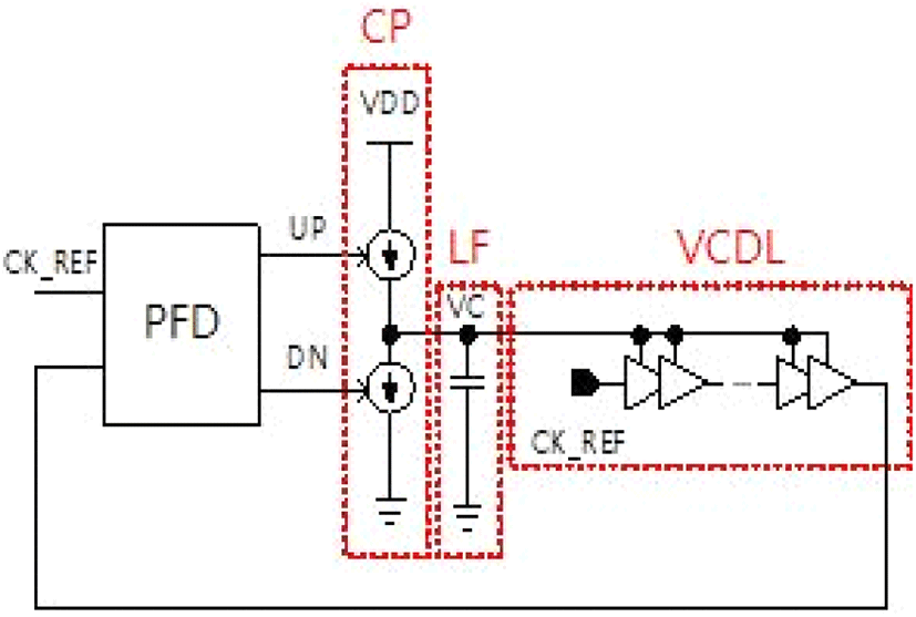
Delay locked loop(DLL)은 high speed microprocessor에서 clock을 생성하거나, digital converter나 mixed signal을 설계할 때, Time calibration을 위한 multiphase clock을 생성하기 위해 사용된다. DLL의 작동 원리는 loop가 닫혀있는 상태에서 negative feedback loop를 통해 random error가 주기마다 누적되지 않기 때문에 PLL보다 적은 jitter를 가진다. 또한 PLL에 비해 구조가 단순하고, 동작 특성상 안정적이며, 소음에 영향을 적게 받는다. DLL은 크게 Analog DLL과 All digital DLL(ADDLL)로 구분된다. 그림 1은 analog DLL의 block diagram이다. Phase detector (PD), charge pump(CP), loop filter(LF)와 voltage controlled delay line(VCDL)으로 구성되어 있으며, analog controlled delay line은 jitter성능이 우수하다. 하지만 lock까지 시간이 많이 걸리고, 소비전력이 크고 LF에 의해 layout size가 크며, 최신 회로에 적용하기가 힘들다. 이러한 단점을 극복하기 위해 Digital DLL[1]이 제안되었다. 높은 Operating frequency와 낮은 전력 소비량은 Digital DLL의 필요성을 느끼게 한다. 최근 Mixed mode ACC-DAC based design[2]에서는 fast lock, low power와 우수한 jitter 성능에 대한 사례가 보고되고 있으며, Accumulator(ACC)의 비활성화로 인해 DAC에서는 lock되어 있는 동안 고정된 값을 출력한다. 그래서 온도나 supply voltage의 변화에 대한 phase error를 detecting이 어렵다. 이러한 단점을 극복하기 위해 Semi digital DLL[1]이 제안되었다. ACC 비활성화로 인해 DAC는 lock 중에 고정값을 가지고 있어 원치 않는 processor나 온도, supply voltage 차이로 인해 lock 이후 phase error를 detecting하기 힘들다.

jkiees-31-7-571-g1
그림 1. | Fig. 1. 기본적인 analog DLL 회로 | Structure of conventional analog DLL.
Download Original Figure

Ⅱ. 본 론

기존의 Semi digital DLL의 경우, VCDL 내부의 delay를 analog signal을 통해 조정할 뿐만 아니라, PVT 변화로 인해 lock 이후 phase error를 검출할 수 없다[1]. 이를 개선하기 위한 DLL구조를 그림 2에 나타내었다. PFD 출력의 UP/DN 신호는 lead하거나 delay 되는 phase 차이를 결정한다. UP/DN 신호에 따라 ACC는 감소하거나 증가하는 시간을 count하게 되고, DCDL 내부의 delay를 조정하게 된다. DLL이 lock이 되면 ACC는 lock detect 회로에 의해 비활성화되고, 고정된 digital code를 출력하게 된다. 즉, DCDL 내부의 delay는 고정되게 된다. lock 이후 PVT 보상을 위한 회로는 원치 않는 processor나 온도, supply voltage 의 변화로 인한 phase error를 지속적으로 check해야 한다. PVT 보상을 위한 회로가 phase error를 검출하고, ACC가 delay를 다시 설정하고 phase error를 취소하여 loop를 다시 lock시킨다. ACC는 높은 주파수에서 전력소모가 심한 Block이다. 전력 소모 감소와 DCDL의 총 delay가 최대일 때, 1주기안에 모든 단계를 커버하기 위해 reference clock을 8분주한 뒤 ACC에 적용하여 낮은 주파수를 가져가 ACC의 전력 소모를 줄이게 한다. 그림 3은 제안된 DLL의 타이밍도이다.

jkiees-31-7-571-g2
그림 2. | Fig. 2. 제안하는 ADDLL의 구조 | Structure of proposed all digital DLL.
Download Original Figure
jkiees-31-7-571-g3
그림 3. | Fig. 3. 제안하는 DLL의 timing diagram | Timing diagram of the proposed ADDLL.
Download Original Figure

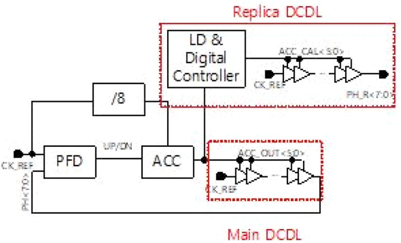
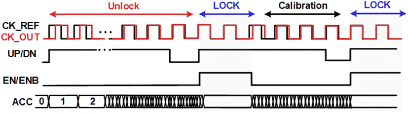
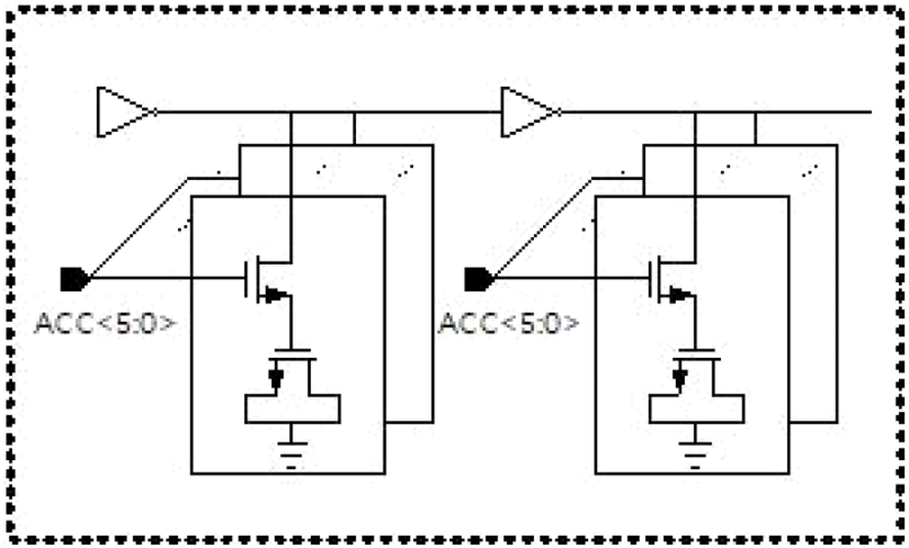
그림 4는 제안된 Digitally controlled delay cell이다. 여기서 2개의 인버터는 Binary weighted switches와 MOS capacitor로 계단 형식으로 구현된다. ACC의 binary 출력은 각 인버터의 출력에서 등가 capacitance를 증가시키거나 감소시켜 delay를 조정한다. Mismatch를 줄이기 위해 binary weighted transistor는 layout을 진행할 때 중심점을 기준으로 병렬로 구현한다.

jkiees-31-7-571-g4
그림 4. | Fig. 4. 제안하는 digital controlled delay cell 회로 | Structure of proposed digital controlled delay cell.
Download Original Figure

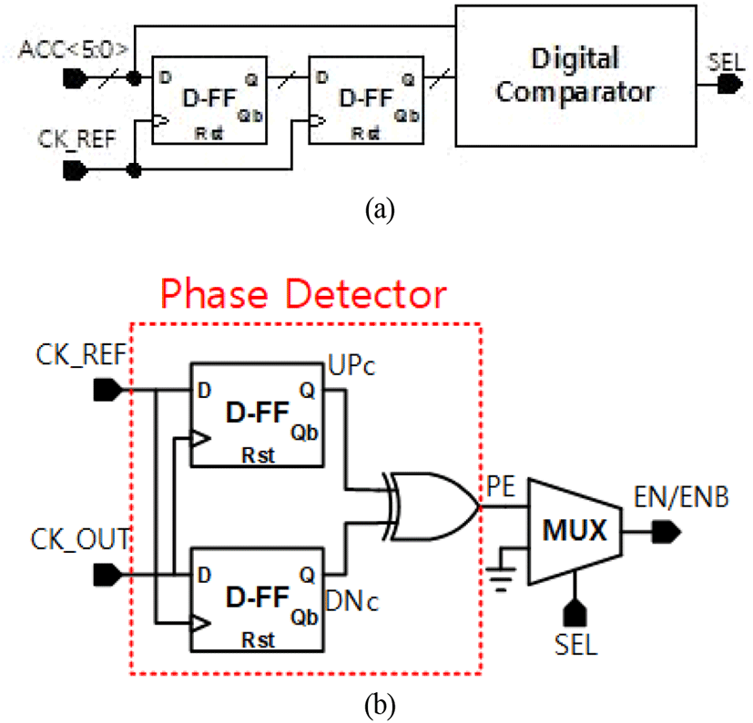
Lock 상태에서는 CK_REF와 CK_OUT의 위상 차이가 1LSB로 제한되고, ACC는 Periodical pattern(n, n+1, n, n+1, …)을 갖는다. 그림 5(a)와 같이 하나의 LSB error를 제거하기 위해 ACC의 출력은 두 번 이동한 다음 비교된다. ACC 값과 shift된 값이 같은 경우, SEL과 PE신호는 각각 ‘1’과 ‘0’ 이된다. 따라서 CK_ACC는 참고문헌 [3]에서 제안된 것과 같이 비활성화된다. 그림 5(b)에서 제안된 PVT 보상 회로는 간단한 PD와 MUX로 구현된다. 이 block에 의해 lock이 되기 전 phase error detecting을 비활성화 되도록 SEL 신로를 ‘0’으로 설정하고, 주 PFD는 phase error를 detecting한다. Lock 이후 phase error가 발생하면 PE신호가 ‘1’이 된다. Simple phase detector는 ACC를 활성화 시킨다. 앞에서 말한 바와 같이 Current consumption과 stability 문제를 줄이기 위해 CK_REF를 8분주한 뒤 ACC에 적용한다.

jkiees-31-7-571-g5
그림 5. | Fig. 5. (a) Lock detector의 구조, (b) PVT 보상회로 구조 | (a) Structure of lock detector, (b) PVT compensation unit.
Download Original Figure

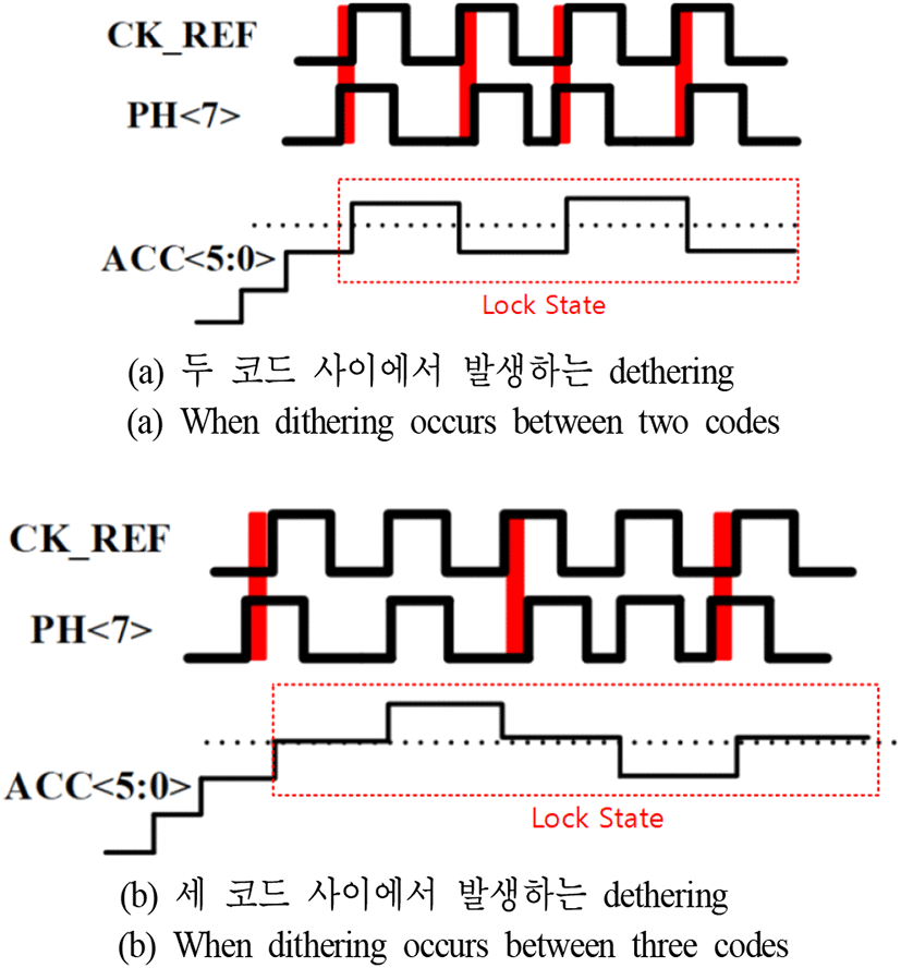
또한 Lock 이후 phase detector로 들어오는 두 신호 CK_ REF와 DCDL의 출력이 동일하게 들어오게 되면 lock state를 중심으로 dithering 현상이 발생한다. 이 현상이 발생하면 ACC 출력이 두 코드(±1 LSB) 사이를 왔다 갔다 하며, 그림 6(a)와 같이 ADDLL의 jitter를 증가시킨다. 또 PD의 Zero dead zone으로 인해 또 다른 error가 발생한다. Dithering 현상을 제거하고, jitter를 줄이기 위해서는 ACC의 출력값을 고정하고, DCDL 내부의 delay가 조정되지 않도록 유지해야 한다. Loop detecting에서 그림 6(a)의 경우, ACC 출력 패턴이 두 코드(n, n+1, n, n+1, n, …)사이에서 검출될 때의 timing diagram이고, 그림 6(b)의 경우, ACC 출력 패턴이 세 코드(n-1, n, n+1, n, n-1, n, n+1, …)사이에서 검출될 때의 timing diagram이다.

jkiees-31-7-571-g6
그림 6. | Fig. 6. Lock state를 중심으로 생기는 dethering 현상 | Dithering of ACC around the lock.
Download Original Figure

Ⅲ. 시뮬레이션 결과 및 분석

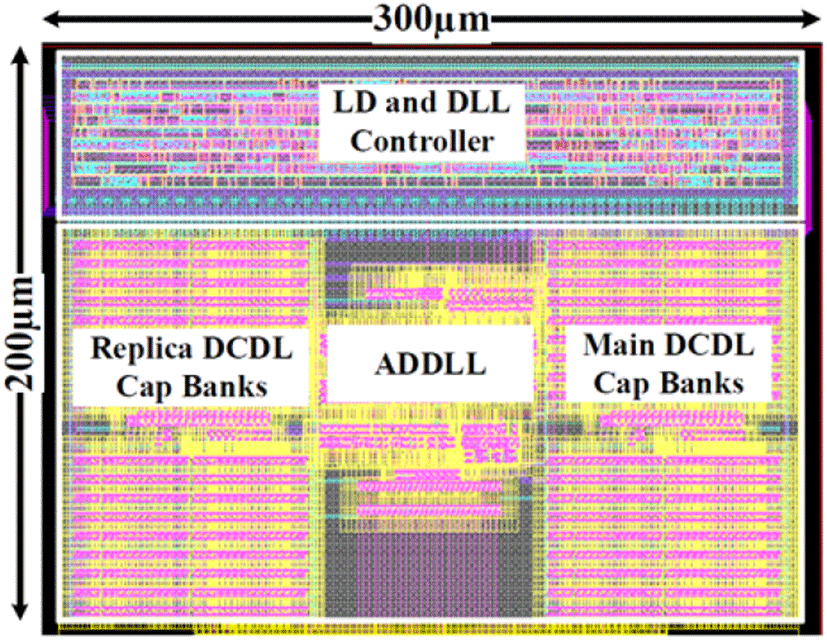
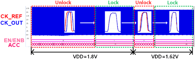
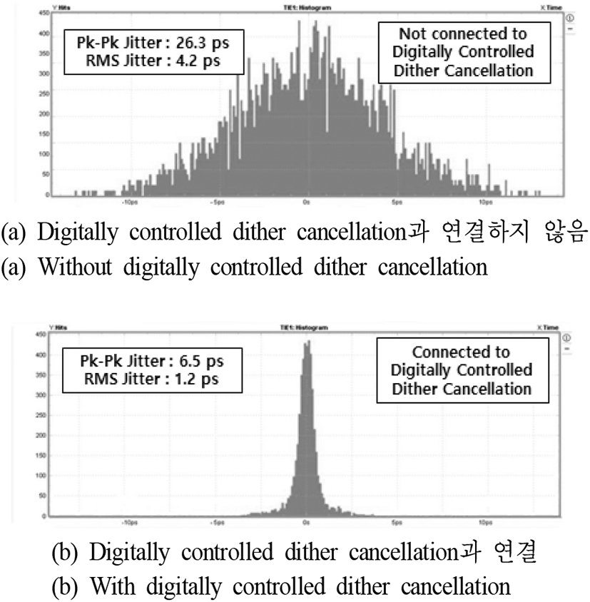
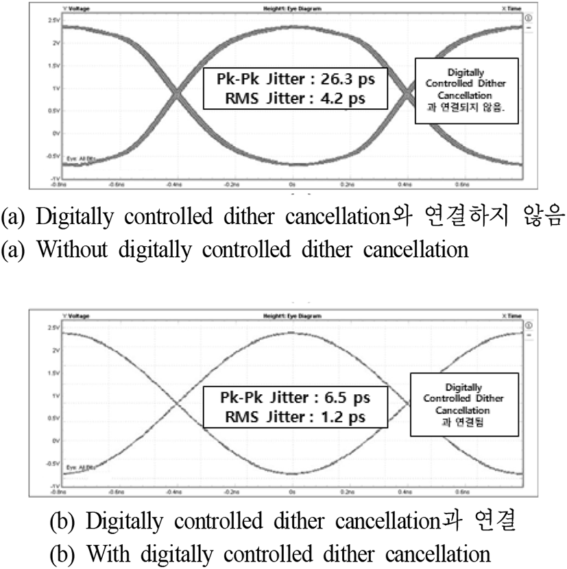
제안하는 ADDLL 회로는 그림 7과 같이 180 nm 표준 CMOS 공정에서 250×300 μm의 사이즈로 설계되었다. 625 MHz의 operating frequency와 1.8 V의 supply voltage에 전류를 6.5 mA를 소비한다. 시뮬레이션 결과는 그림 8에 나타나 있다. ACC 패턴에 따라 ADDLL 회로가 lock이 되는지 확인한다. Lock 이후 PVT 변동을 모델링하기 위해 VDD를 10 % 감소시켜 1.8~1.62 V까지 변화를 주어 확인한다. VDD variation 이후 PD에 의해 phase error가 감지되고, ACC가 패턴을 따르지 않는다. 따라서 ADDLL의 close loop와 ACC 값 update에 의해 생성된 phase error가 사라진다. 측정 결과, digitally controlled dither cancellation과 결합하기 전 peak to peak jitter는 26.3 ps이고, RMS jitter는 4.2 ps이다. Digitally controlled dither cancellation 결합 후 peak to peak jitter는 6.5 ps이고, RMS jitter는 1.2 ps이다. 그림 9(a)는 digitally controlled dither cancellation과 연결하지 않은 상태로 ADDLL의 jitter특성을 측정한 것이고, 그림 9(b)는 digitally controlled dither cancellation과 연결하고 측정한 데이터이다. 그림 10(a)는 Digitally controlled dither cancellation과 연결한 상태로 측정한 eye diagram이고, 그림 10(b)는 digitally controlled dither cancellation과 연결하고, 측정한 eye diagram이다. 표 1은 다른 최근 논문과 요약 비교한 표이다.

jkiees-31-7-571-g7
그림 7. | Fig. 7. 제안하는 ADDLL의 layout pattern. | Layout pattern of the proposed ADDLL.
Download Original Figure
jkiees-31-7-571-g8
그림 8. | Fig. 8. Lock 이후 VDD 변화에 따른 출력 변화 결과 | Simulation result with applying VDD variation after lock.
Download Original Figure
jkiees-31-7-571-g9
그림 9. | Fig. 9. ADDLL의 jitter 특성의 측정결과 | Measurement of ADDLL jitter characteristic.
Download Original Figure
jkiees-31-7-571-g10
그림 10. | Fig. 10. ADDLL의 jitter 특성을 나타낸 eye diagram | Measurement result for jitter characteristic.
Download Original Figure
표 1. | Table 1. 성능 비교 | Performance comparision.
Parameter Recent designs
This work Ref [2] Ref [4]
Process 180 nm 180 nm 130 nm
Power supply 1.8 V 1.8 V 1.5 V
Area (mm2) 0.075 NA 0.08
Power consumption (mW) 12 @ 625 MHz 7.85 @ 625 MHz 26 @ 180 MHz
Operating frequency (MHz) 350-900 20-625 80-450
Download Excel Table

Ⅳ. 결 론

본 논문에서는 Analog DLL의 누설 전류 문제와 PVT 변화에 따른 phase error를 제거하기 위한 replica DCDL을 이용한 ADDLL을 제안하였다. 제안된 구조는 main DCDL에서 delay를 추적하여 lock 이후 PVT 변화가 발생시 phase error를 추적하도록 replica DCDL이 구동되는 LD와 digital controller를 제안하였다.

Acknowledgements

이 논문은 2014년도 정부(미래창조과학부)의 재원으로 한국연구재단의 지원을 받아 수행된 기초연구사업임(2014R1A5A1011478).

References

[1].

C. Portmann, A. Chu, N. Hays, S. Sidiropoulos, D. Stark, and P. Chau, et al., “A multiple vendor 2.5-V DLL for 1.6-GB/s DRAMs,” in 1999 Symposium on VLSI Circuits. Digest of Papers, Kyoto, Jun. 1999, pp. 153- 156.

[2].

A. Hejazi, S. Kazeminia, and R. Abdollahi, “A digitally assisted 20 MHz~600 MHz 16-phase DLL enhanced with dynamic gain control loops,” in 2015 European Conference on Circuit Theory and Design(ECCTD), Trondheim, Aug. 2015, pp. 1-4.

[3].

S. Kazeminia, R. Abdollahi, and A. Hejazi, “A fast- locking low-jitter digitally-enhanced DLL dynamically controlled for loop-gain and stability,” Analog Integrated Circuits and Signal Processing, vol. 94, no. 3, pp. 507- 517, 2018.

[4].

D. Zhang, H. G. Yang, W. Zhu, W. Li, Z. Huang, and L. Li, “A multiphase DLL with a novel fast-locking fine-code time-to-digital converter,” IEEE Transactions on Very Large Scale Integration(VLSI) Systems, vol. 23, no. 11, pp. 2680-2684, Nov. 2015.

Author Information

박 건 호 [성균관대학교/석사과정]

jkiees-31-7-571-i1

  • 2015년: 동아대학교 전자공학과 (공학사)

  • 2019년~현재: 성균관대학교 전자전기공학부 석사과정

  • [주 관심분야] 아날로그 IC, 아날로그-디지털 혼성모드 VLSI 시스템 설계

이 재 진 [성균관대학교/석사과정]

jkiees-31-7-571-i2

  • 2018년: 한동대학교 전자공학과 (공학사)

  • 2018년~현재: 성균관대학교 전자전기공학부 석사과정

  • [주 관심분야] CMOS RF Transceiver

오 성 진 [성균관대학교/박사과정]

jkiees-31-7-571-i3

  • 2014년: 성균관대학교 전자전기공학과 (공학사)

  • 2014년~현재: 성균관대학교 전자전기공학부 석박통합

  • [주 관심분야] CMOS RF Transceiver, ADPLL, Wireless Power Transfer Receiver, and Rectifier

이 강 윤 [성균관대학교/교수]

jkiees-31-7-571-i4

  • 1996년: 서울대학교 전기공학부 (공학사)

  • 1998년: 서울대학교 전기공학과 (공학석사)

  • 2003년: 서울대학교 전자공학과 (공학박사)

  • 2005~2011년: 건국대학교 전기전자공학과 교수

  • 2018년~현재: 성균관대학교 전자전기공학과 교수

  • [주 관심분야] CMOS RF Transceiver, 아날로그 IC, 아날로그-디지털 혼성모드 VLSI 시스템 설계